Nonvolatile memory cell and method for fabricating the same

a memory cell and non-volatile technology, applied in the direction of semiconductor devices, electrical apparatus, transistors, etc., can solve the problems of inability to meet the requirements of inability to achieve high density memory devices. achieve the effect of reducing cell size and stable operation reliability

Active Publication Date: 2010-10-28
KEY FOUNDRY CO LTD
View PDF18 Cites 25 Cited by
  • Summary
  • Abstract
  • Description
  • Claims
  • Application Information

AI Technical Summary

Benefits of technology

[0014]An embodiment of the present invention is directed to providing a nonvolatile memory cell and a method for fabricating the same, capable of securing stable operational reliability as well as reducing a cell size.
[0015]Another embodiment of the present invention is directed to providing a nonvolatile memory cell and a method for fabricating the same, capable of increasing a coupling ratio and thus reducing a driving voltage.

Problems solved by technology

However, the stack gate may induce several problems when implementing a complicated operation by its simple construction.
Accordingly, in low density products, a small size of the memory cell may not be an advantage anymore.
The split gate is widely used by its excellencies of the operational reliability although it is not appropriate for a high density memory device by its great cell size.
However, since the size of a cell including the split gate is great, there are many difficulties to apply the split gate to the high density memory device.

Method used


Image

  • Nonvolatile memory cell and method for fabricating the same
  • Nonvolatile memory cell and method for fabricating the same
  • Nonvolatile memory cell and method for fabricating the same

Examples


first embodiment

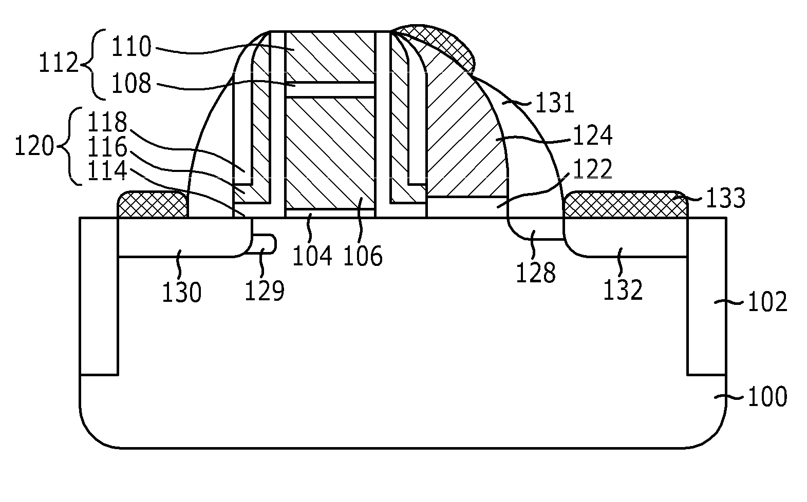
[0045]FIG. 4 illustrates a plane view of a nonvolatile memory cell in accordance with the present invention. FIG. 5 illustrates a cross-sectional view taken along a line I-I′ described in FIG. 4. Even though a silicide layer 133 formed on a control gate 124 shown in FIG. 5 is also formed on the control gate 124 described in FIG. 4, it is not illustrated in FIG. 4 for the simplicity of explanation.

[0046]Referring to FIGS. 4 and 5, the nonvolatile memory cell in accordance with the first embodiment of the present invention includes the control gate 124 that is formed on a dielectric layer 120 to cover at least one sidewall of a floating gate 106. Preferably, the control gate 124 is formed on the dielectric layer 120 to cover one of both sidewalls existing on a uniaxial plane of the floating gate 106, e.g., in a Y axial direction in FIG. 4. Furthermore, the control gate 124 is formed in a direction that a source region 132 is formed.

[0047]The nonvolatile memory cell in accordance with ...

second embodiment

[0086]FIG. 11 illustrates a plane view of a nonvolatile memory cell in accordance with the present invention. FIG. 12 illustrates a cross-sectional view taken along a line I-I′ described in FIG. 11. Even though a silicide layer 228 formed on a control gate 224A shown in FIG. 12 is also formed on the control gate 224A described in FIG. 11, it is not illustrated in FIG. 11 for the simplicity of explanation.

[0087]Referring to FIGS. 11 and 12, unlike in the first embodiment of the present invention, the nonvolatile memory cell in accordance with the second embodiment of the present invention includes the control gate 224A formed to overlap with both sidewalls of a floating gate 206 in a Y axial direction. As described in the first embodiment of the present invention, if the control gate is formed to overlap with one sidewall of the floating gate in the Y axial direction, there is an advantage of increasing a degree of integration of the device, whereas there is a limitation in increasin...

third embodiment

[0103]FIG. 14 illustrates a plane view of a nonvolatile memory cell in accordance with the present invention.

[0104]Referring to FIG. 14, the nonvolatile memory cell in accordance with the third embodiment includes a concavo-convex part 307 formed on a surface, i.e., the outer circumference, of a floating gate 306 to increase a coupling ratio of the cell by increasing a junction area between the floating gate 306 and a control gate 324. Preferably, the concavo-convex part 307 is formed to overlap with the control gate 324. Since other components than the floating gate 306, e.g., a drain region, a source region, etc., are formed in the same manner as those in accordance with the first and second embodiments, the detailed description thereof will be omitted herein. Meanwhile, a reference numeral 328 represents a silicide layer and a reference numeral 318 depicts a dielectric layer.

[0105]In accordance with the third embodiment of the present invention, the concavo-convex part 307 is for...


PUM


Abstract

A nonvolatile memory cell and a method for fabricating the same can secure stable operational reliability as well as reducing a cell size. The nonvolatile memory cell includes a drain region formed in a substrate, a source region formed in the substrate to be separated from the drain region, a floating gate formed over the substrate between the drain region and the source region, a halo region formed in the substrate in a direction that the drain region is formed, a dielectric layer formed on sidewalls of the floating gate, and a control gate formed over the dielectric layer to overlap with at least one sidewall of the floating gate.

Description

CROSS-REFERENCE TO RELATED APPLICATIONS[0001]The present invention claims priority of Korean Patent Application No. 10-2009-0011908 filed on Feb. 13, 2009 which is incorporated herein by reference in its entirety.BACKGROUND OF THE INVENTION[0002]1. Field of the Invention[0003]The present invention relates to a nonvolatile memory device and a method for fabricating the same, and more particularly, to a nonvolatile memory cell and a method for fabricating the same.[0004]2. Description of Related Art[0005]Since a nonvolatile memory device maintains data stored in memory cells even when power to the device is turned off, it is used in various applications and its importance is also increasing. As representative nonvolatile memory devices, a flash memory device and an electrical erasable programmable read only memory (EEPROM) device are well known.[0006]A cell of the nonvolatile memory device, i.e., a nonvolatile memory cell, may be classified into a split gate structure and a stack gate...

Claims


Application Information

Patent Timeline
Patent Type & Authority Applications(United States)
IPC IPC(8): H01L29/788H01L21/336
CPCH01L21/28273H01L29/42324H01L29/7881H01L29/66825H01L29/512H01L29/40114H01L21/265
Inventor CHOI, TAE-HOLEE, JUNG-HWANHONG, HEUNG-GEECHO, JEONG-HOCHOO, MIN-WANHAN, IL-SEOK
Owner KEY FOUNDRY CO LTD
Why Eureka
Try Eureka