Voltage converter
- Summary
- Abstract
- Description
- Claims
- Application Information
AI Technical Summary
Benefits of technology
Problems solved by technology
Method used
Image
Examples
Embodiment Construction
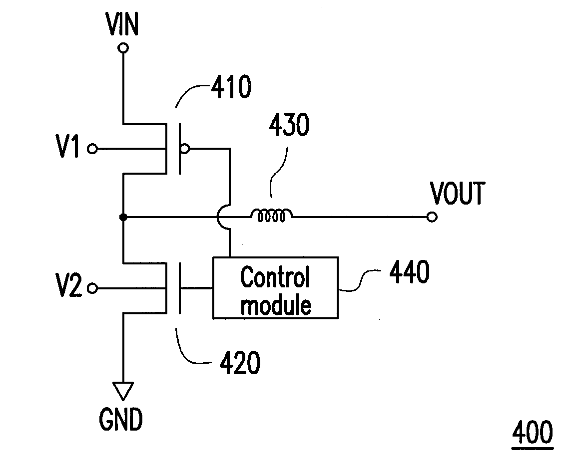
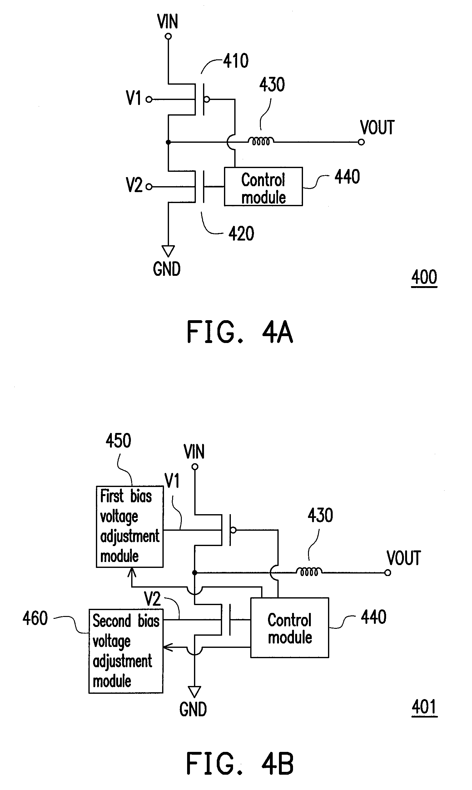
[0029]FIG. 4A is a schematic diagram illustrating a voltage converter of an exemplary embodiment of the present invention. Referring to FIG. 4A, the voltage converter 400 includes a first transistor 410, a second transistor 420, an inductor 430 and a control module 440.
[0030]A source terminal of the first transistor 410 receives the input voltage VIN, and a body terminal of the first transistor 410 receives a first bias voltage V1. A drain terminal of the second transistor 420 is coupled to the sink terminal of the first transistor 410, a source terminal of the second transistor 420 is coupled to the ground terminal GND, and a body terminal of the second transistor 420 receives a second bias voltage V2. The inductor 430 has a first terminal coupled to the drain terminal of the first transistor 410 and a second terminal generating an output voltage VOUT. The control module 440 is coupled to a gate terminal of the first transistor 410 and a gate terminal of the second transistor 420 f...
PUM
 Abstract
Description
Claims
Application Information


