Liquid crystal display device

a liquid crystal display and display panel technology, applied in the direction of static indicating devices, instruments, other domestic articles, etc., can solve the problems of mechanical strength problem, reduced thickness of liquid crystal display panels, and difficulty in obtaining such standardized glass substrates from a market, so as to achieve high reliability reduce the thickness of liquid crystal display devices

Active Publication Date: 2010-10-28
PANASONIC LIQUID CRYSTAL DISPLAY CO LTD +1
View PDF7 Cites 27 Cited by
  • Summary
  • Abstract
  • Description
  • Claims
  • Application Information

AI Technical Summary

Benefits of technology

[0021]According to the present invention, no peeling stress is applied to the adhesive sheet, even if the thickness of the adhesive sheet for bonding the front window and the touch panel is smaller than the thickness of the touch-panel flexible wiring substrate and the thickness of the logo formed on the front window. As a result, it is possible to provide a highly reliable liquid cry

Problems solved by technology

It is difficult to obtain such standardized glass substrates from a market.
In addition, very thin glass substrates have a problem relating to mechanical strength and bending in the production process, leading to a reduction in the production yield.
The reduction of the thickness of the liquid crystal display panel poses a problem of the mechanical strength.
When a mechanical pressure is applied to the display surface of the liquid crystal display panel, there is a risk that the liquid crystal display panel will be broken.
If a thick printed mark is formed betw

Method used


Image

  • Liquid crystal display device
  • Liquid crystal display device
  • Liquid crystal display device

Examples


first embodiment

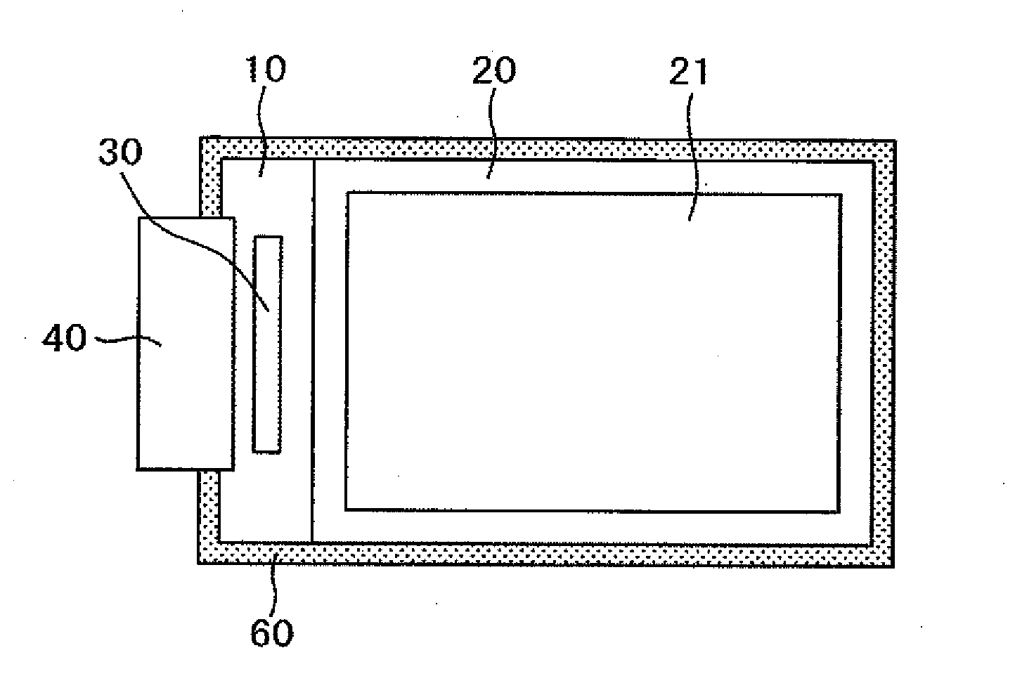
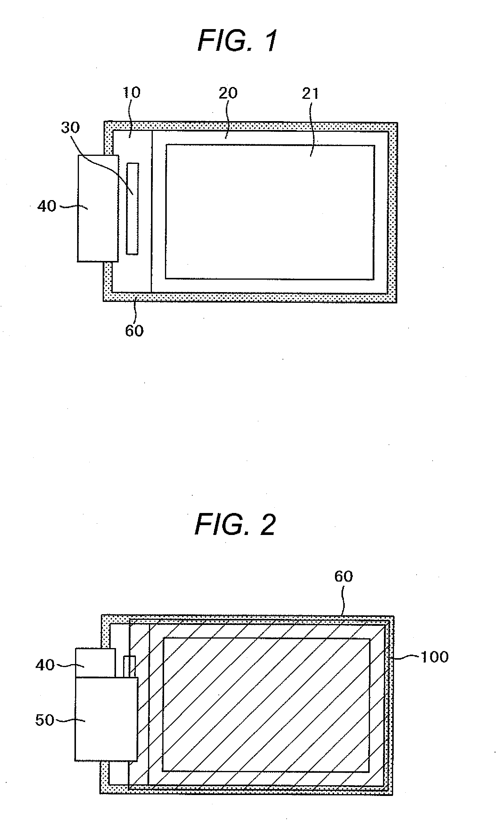
[0034]FIG. 1 is a top view of a liquid crystal display device used for mobile phones or other electronic devices, according to the present invention. In FIG. 1, a color filter substrate 20 is mounted to a TFT substrate 10. A liquid crystal layer, not shown, is interposed between the TFT substrate 10 and the color filter substrate 20. The TFT substrate 10 and the color filter substrate 20 are bonded together with a sealing material, not shown, which is formed in the frame portion of the liquid crystal display panel. The TFT substrate 10 is made to be larger than the color filter substrate 20. A terminal portion is formed in the portion of the TFT substrate 10 extending beyond the color filter substrate 20, in order to supply power, image signals, scan signals, and the like.

[0035]An IC driver 30 is connected to the terminal portion to drive scan lines, image lines, and the like. The IC driver 30 includes a scan line drive circuit and an image signal line drive circuit. The IC driver 3...

second embodiment

[0070]When the light from the light emitting diode of the backlight is input to the logo 80 formed on the back side of the front window 200, a predetermined design quality may not be obtained in terms of the color or other optical characteristics of the logo 80. In order to prevent this, in the first embodiment, the thickness of the second layer 82 of the logo 80 is increased. However, the light shielding effect may not be sufficiently obtained in the first embodiment. In a second embodiment, a third layer 83, which is a light shielding film, is further formed on the second layer 82 for forming white or a predetermined color of the logo 80, in order to prevent the effect of the light from the light emitting diode.

[0071]FIGS. 8A, 8B, and 8C are cross-sectional views of the process of forming the logo 80 according to the second embodiment. FIG. 8A is a view in which the first layer 81 is formed on the back surface of the front window 200. FIG. 8B is a view in which the second layer 82...

third embodiment

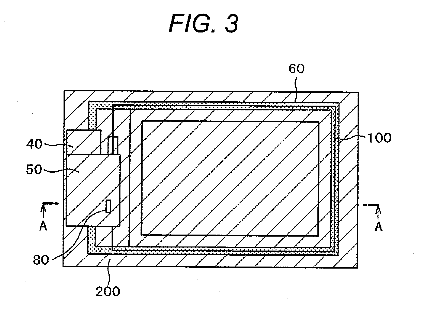
[0078]In the first embodiment, the distance L between the end portion of the second layer 82 of the logo 80 and the end portion of the touch panel 100 is set to be greater than zero. In the second embodiment, the distance L between the end portion of the three layers of the logo 80 and the end portion of the touch panel 100 is set to be greater than zero. In the vicinity of the distance L of zero, the bending stress is large. If the relationship d12+d3 is established in FIG. 7 and other figures, there may be a peeling stress on the adhesive sheet 210 between the front window 200 and the touch-panel flexible wiring substrate 50.

[0079]A third embodiment deals with this problem. FIG. 10 is a detailed cross-sectional view around the logo 80 formed on the back surface of the front window 200 according to the third embodiment. In FIG. 10, the configuration below the touch panel 100 is omitted.

[0080]In FIG. 10, the touch-panel flexible wiring substrate 50 is mounted to the touch panel 100....


PUM


Abstract

In a liquid crystal display device in which a front window and a touch panel are bonded together with an adhesive sheet, a logo having plural layers is formed on a back side of the front window. A touch-panel flexible wiring substrate is mounted to the touch panel. A plane distance between an end portion of the plural layers of the logo and an end portion of the touch panel is set to greater than zero. With this configuration, it is possible to prevent a peeling stress on the adhesive sheet, even if a thickness of the adhesive sheet is smaller than the sum of a thickness of the touch-panel flexible wiring substrate and a thickness of the logo.

Description

CLAIM OF PRIORITY[0001]The present application claims priority from Japanese Patent Application JP 2009-107678 filed on Apr. 27, 2009, the content of which is hereby incorporated by reference into this application.FIELD OF THE INVENTION[0002]The present invention relates to a liquid crystal display device, and more particularly to a small display device having a touch panel and a front window provided in the interfacial surface of the display device for electronic devices such as mobile phones.BACKGROUND OF THE INVENTION[0003]In the liquid crystal display device, a TFT substrate has pixel electrodes and thin film transistors (TFTs), and the like, arranged at a matrix form. A color filter substrate has a color filters arranged at positions corresponding to the pixel electrodes of the TFT substrate. The TFT substrate and the color filter substrate are opposite to each other with a liquid crystal interposed therebetween. In such a configuration, the liquid crystal display device forms ...

Claims


Application Information

Patent Timeline
IPC IPC(8): G06F3/045G09G3/36
CPCG02F1/13338G06F3/041G02F2001/133374G02F1/133374B32B7/12B32B2457/202G06F3/0412G06F2203/04103H04B1/3888H04M1/0266B32B2307/412B32B2457/208
Inventor OOHIRA, EIJI
Owner PANASONIC LIQUID CRYSTAL DISPLAY CO LTD
Why Eureka
Try Eureka