Liquid crystal display device

Active Publication Date: 2008-11-20
SEMICON ENERGY LAB CO LTD
View PDF7 Cites 200 Cited by
  • Summary
  • Abstract
  • Description
  • Claims
  • Application Information

AI Technical Summary

Benefits of technology

[0078]In accordance with the present invention, performance as a display device can be maintained and viewing angle characteristics can be improved compared to that of a conventional display device. Alternatively, in accordance with the present invention, a highly reliable display device can be provided. Alternatively, in accordance with the present invention, a display device having high contrast can be provided. Alternatively, in accordance with the present invention, a lightweight display device can be provided. Alternatively, in acco

Problems solved by technology

However, it cannot be said that viewing angle characteristics are sufficient, and there is a possibility that the viewing angle characteristics can be improved when subpixels are additionally provided.
However, when the number of subpixels is simply increased, disadvantages such as decrease in the aperture ratio and increase of driver circuits occur to increase manufacturing cost and cause an a

Method used


Image

  • Liquid crystal display device
  • Liquid crystal display device
  • Liquid crystal display device

Examples


embodiment mode 1

(Embodiment Mode 1)

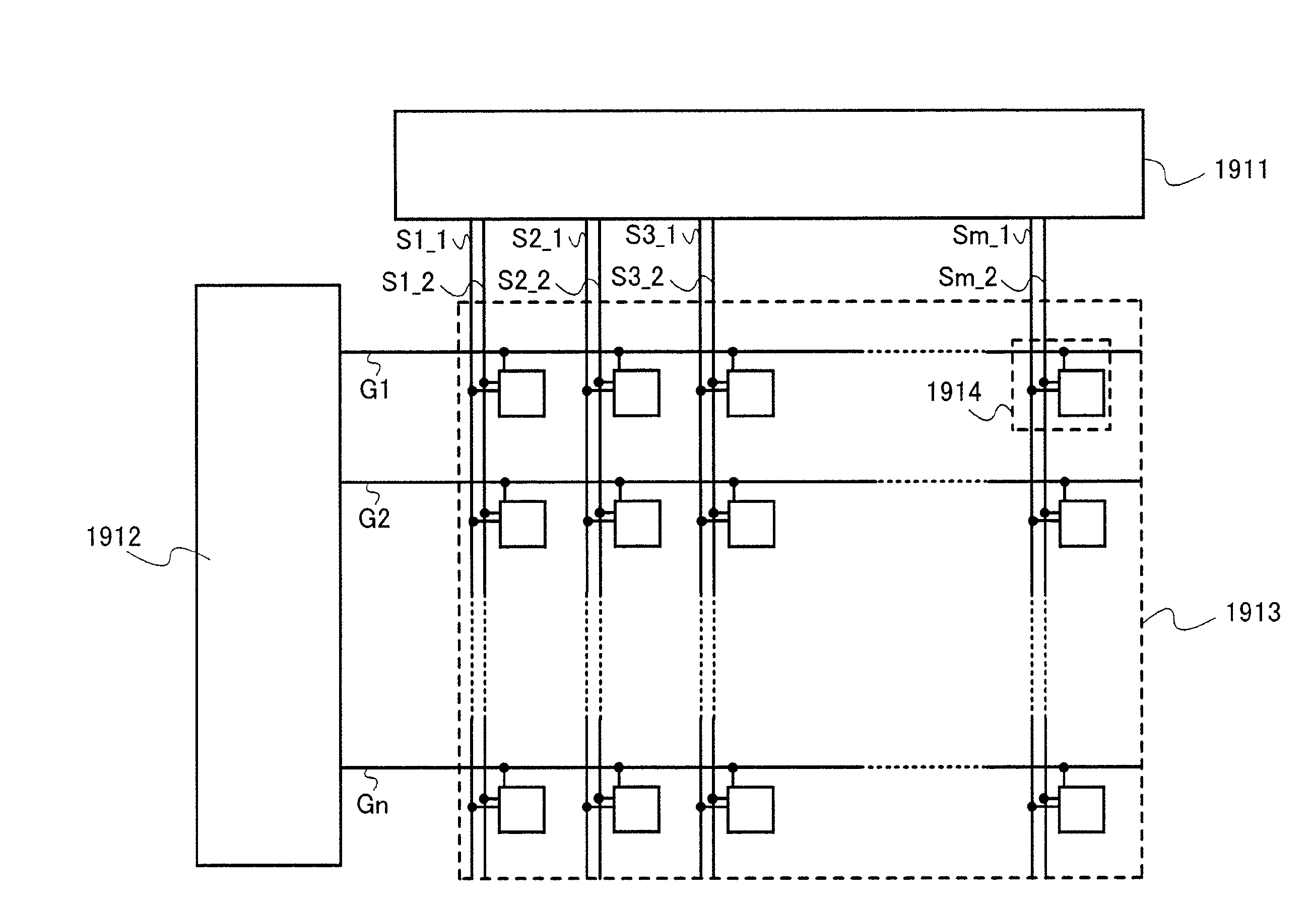
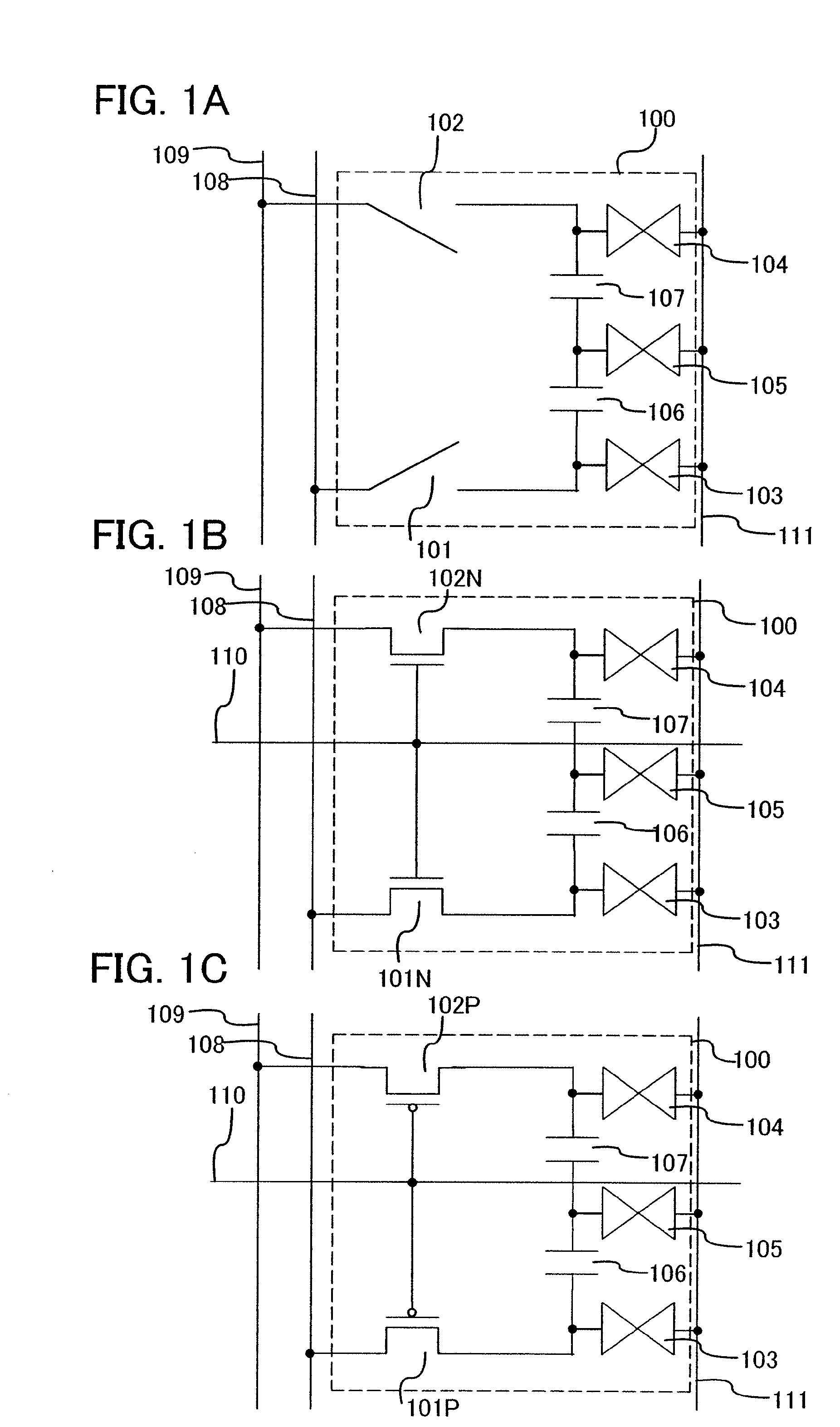
[0225]In this embodiment mode, structures and operations of a pixel circuit included in a liquid crystal display device of the present invention are described with reference to the drawings. The pixel circuit of the liquid crystal display device of the present invention has a structure in which one pixel is provided with a plurality of liquid crystal elements and voltage which is applied is varied between the liquid crystal elements. Specifically, one of or both a capacitor and a resistor connected to a liquid crystal element are provided to vary voltage applied to the liquid crystal element.

[0226]Note that a display element is not limited to a liquid crystal element, and various display elements (e.g., a light-emitting element (an EL element (e.g., an EL element including organic and inorganic materials, an organic EL element, or an inorganic EL element) or an electron emitter), an electrophoresis element, and the like) can be used.

[0227]There are various operati...

embodiment mode 2

(Embodiment Mode 2)

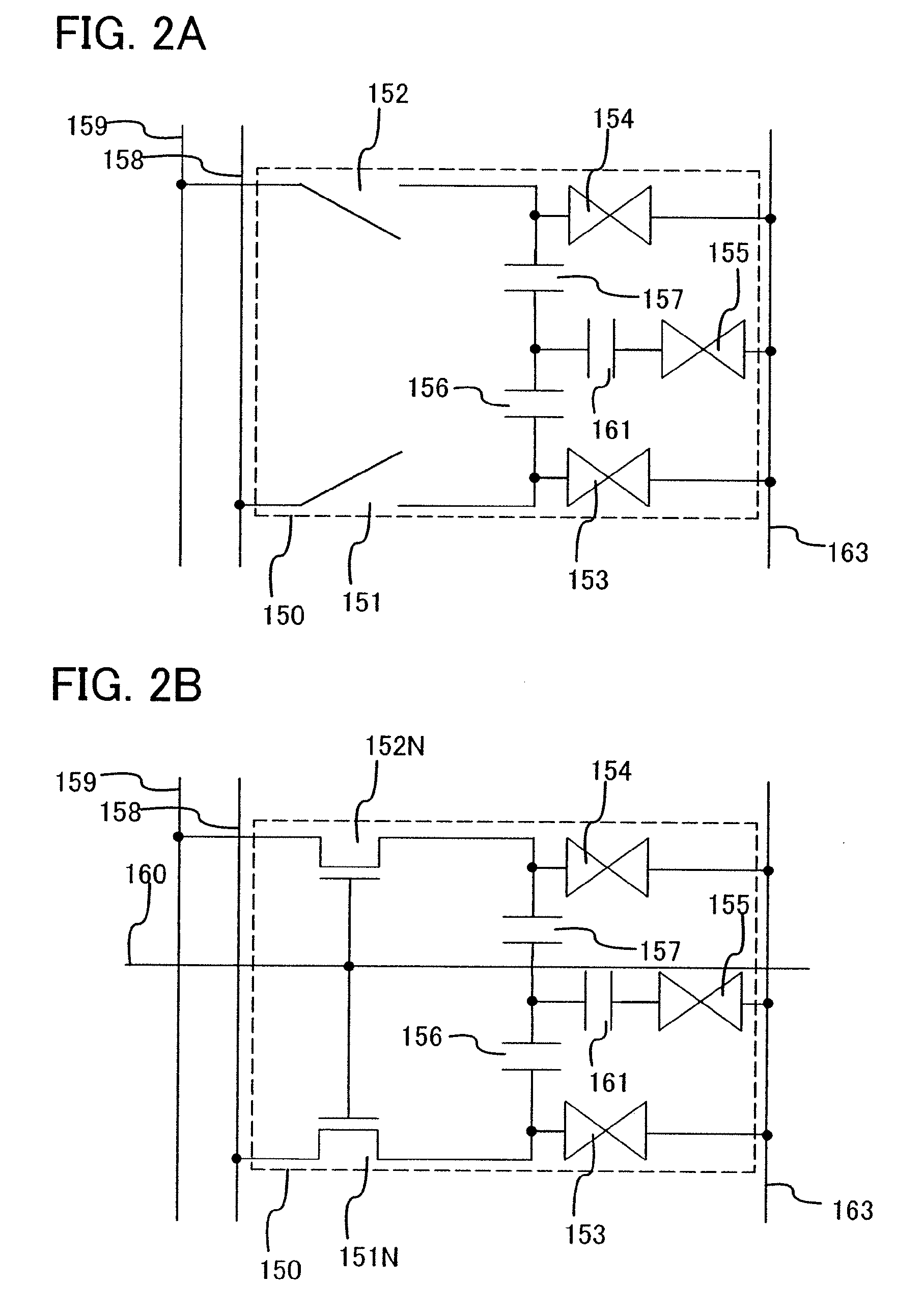
[0380]In Embodiment Mode 1, new voltage is produced by voltage division by using a capacitor and is supplied to a liquid crystal element. Note that an element for producing new voltage is not limited to a capacitor. Various elements such as a divider element, an element which converts current into voltage, a non-linear element, an element having a resistance component, an element having a capacitance component, an inductor, a diode, a transistor, a resistor, and a switch can be used. In addition, when these elements are connected in series or in parallel in combination, a desired circuit can be realized. Such an element is referred to as a divider element.

[0381]FIGS. 23A and 23B show the case where the capacitors in FIGS. 1A to 1C are generalized as divider elements. Therefore, the contents described in Embodiment Mode 1 can also be applied to FIGS. 23A and 23B.

[0382]FIG. 23A shows an example of a structure of a pixel circuit included in a liquid crystal display d...

embodiment mode 3

(Embodiment Mode 3)

[0502]In this embodiment mode, a structure and a manufacturing method of a transistor are described.

[0503]FIGS. 51A to 51G are cross-sectional views showing examples of a structure and a manufacturing method of a transistor. FIG. 51A is a cross-sectional view showing a structural example of the transistor. FIGS. 51B to 51G are cross-sectional views showing an example of a manufacturing method of the transistor.

[0504]Note that the structure and the manufacturing method of the transistor are not limited to those shown in FIGS. 51A to 51G, and various structures and manufacturing methods can be used.

[0505]First, structural examples of transistors are described with reference to FIG. 51A. FIG. 51A is a cross-sectional view of a plurality of transistors each having a different structure. Here, in FIG. 51A, the plurality of transistors each having a different structure are arranged, which is for describing the structures of the transistors. Accordingly, it is not necess...


PUM


Abstract

To improve viewing angle characteristics by varying voltage which is applied between liquid crystal elements. A liquid crystal display device in which one pixel is provided with three or more liquid crystal elements and the level of voltage which is applied is varied between the liquid crystal elements is varied. In order to vary the level of the voltage which is applied between the liquid crystal elements, an element which divides the applied voltage is provided. In order to vary the level of the applied voltage, a capacitor, a resistor, a transistor, or the like is used. Viewing angle characteristics can be improved by varying the level of the voltage which is applied between the liquid crystal elements.

Description

BACKGROUND OF THE INVENTION[0001]1. Field of the Invention[0002]The present invention relates to an object, a method, or a method for producing an object. In particular, the present invention relates to a display device or a semiconductor device, particularly relates to a display device. Specifically, the present invention relates to an active matrix liquid crystal display device.[0003]2. Description of the Related Art[0004]In recent years, a liquid crystal display device and an EL display device have been actively developed as a display device. In particular, a liquid crystal display device has been remarkably spread. In a liquid crystal display device, high contrast, high-speed response, a wide viewing angle, and the like are necessary. Further, in a liquid crystal display device which is mounted on a portable electronic device, reduction in power consumption, weight, and size is also an important object.[0005]In order to widen the viewing angle of a liquid crystal display device,...

Claims


Application Information

Patent Timeline
IPC IPC(8): G02F1/133
CPCG02F1/13624G02F1/136213G02F2001/136295G09G3/2022G09G3/3233G09G3/3648G09G3/3659G09G2300/0443G09G2300/0447G09G2300/0809G09G2300/0842G09G2300/0852G09G2310/0262G09G2320/0252G09G2320/0261G09G2320/028G09G2320/10G09G2320/106G09G2330/021G09G2340/0435G09G2340/16H01L27/12G02F2001/134345G02F1/134345G02F1/136295G02F1/136227G02F1/136286G02F1/1368
Inventor KIMURA, HAJIME
Owner SEMICON ENERGY LAB CO LTD
Why Eureka
Try Eureka