

Method for Manufacturing Display Device
a display device and manufacturing method technology, applied in the direction of identification means, instruments, non-linear optics, etc., can solve the problems of stacking of insulating layers, reduce the complexity of photolithography process, reduce the loss of materials, and improve the effect of image quality
- Summary
- Abstract
- Description
- Claims
- Application Information
AI Technical Summary
Benefits of technology
Problems solved by technology
Method used
Image

Examples
embodiment mode 1
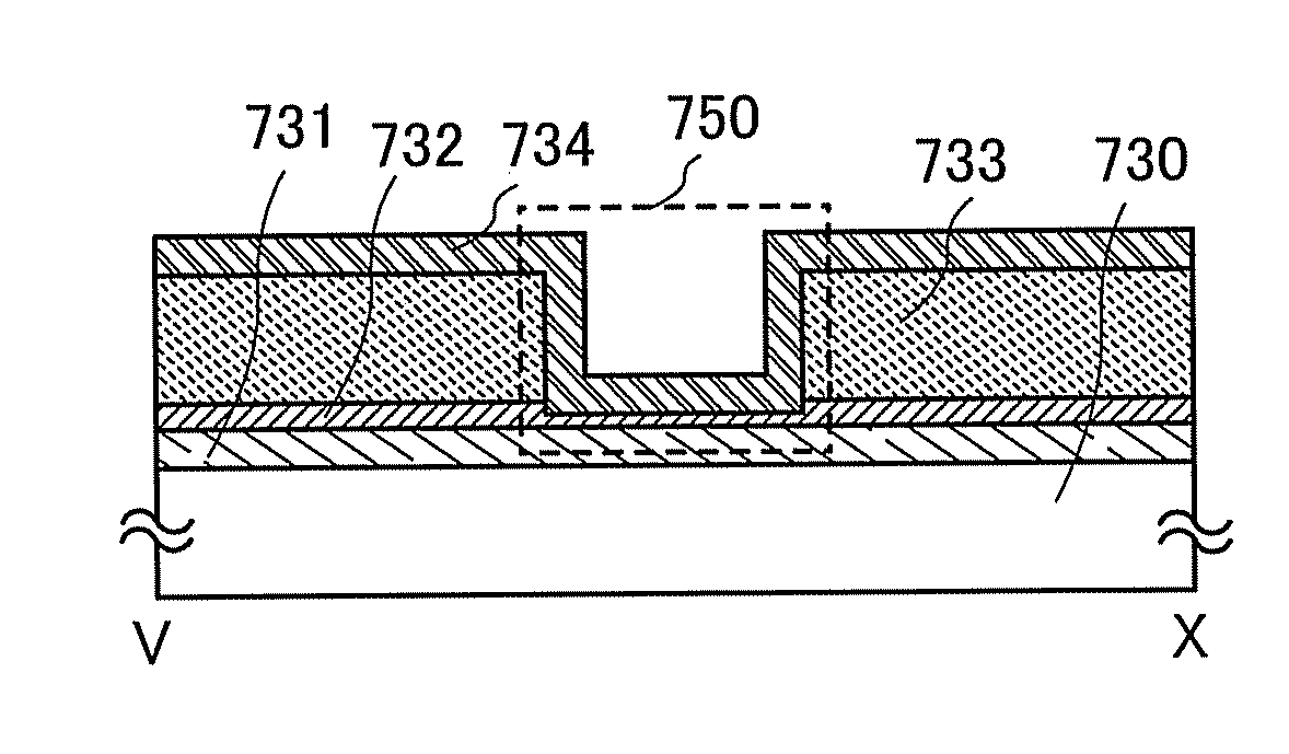
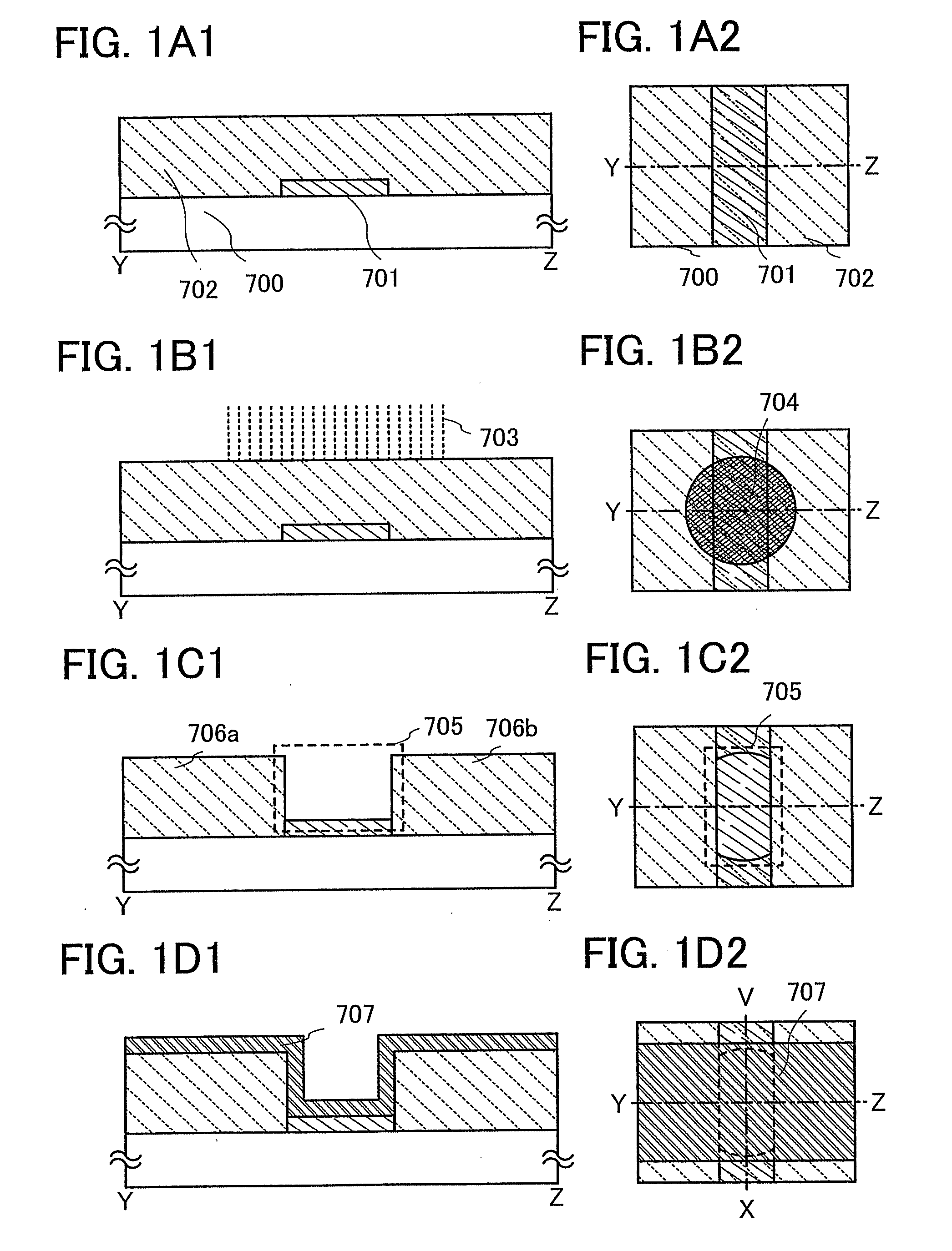
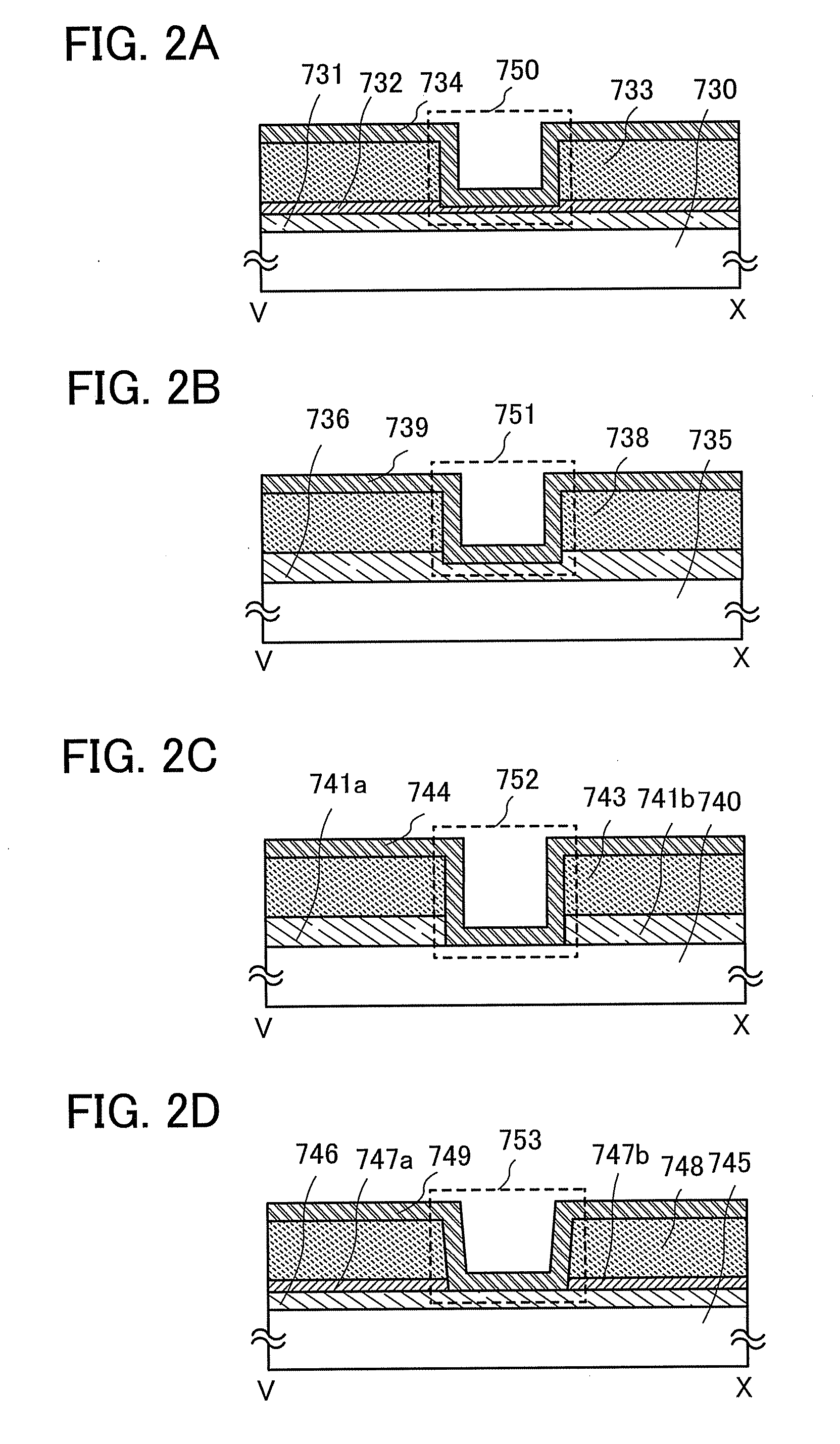
[0055]In this embodiment mode, a method for forming a contact hole in order to manufacture a display device at low cost through a highly reliable, more simplified process is described with reference to FIGS. 1A1 and 1A2, 1B1 and 1B2, 1C1 and 1C2, and 1D1 and 1D2.
[0056]In the case where thin films (each of which is a conductive layer or a semiconductor layer) which are stacked with an insulating layer interposed therebetween are electrically connected to each other, an opening (a so-called contact hole) is formed in the insulating layer. In this case, a mask layer is not formed over the insulating layer, and the opening is selectively formed by laser light irradiation. After a light-absorbing layer which absorbs irradiated light is formed and an insulating layer is stacked over the light-absorbing layer, a region at which an opening is to be formed in the stacked layer of the light-absorbing layer and the insulating layer is irradiated with laser light from the insulating layer side....
embodiment mode 2
[0092]In this embodiment mode, a method for forming a contact hole in order to manufacture a display device at low cost through a highly reliable, more simplified process is described with reference to FIGS. 4A1, 4A2, 4B1, 4B2, 4C1, 4C2, 4D1, and 4D2.
[0093]In the case where thin films (each of which is a conductive layer or a semiconductor layer) which are stacked with an insulating layer interposed therebetween are electrically connected to each other, an opening (a so-called contact hole) is formed in the insulating layer. In this case, a mask layer is not formed over the insulating layer, and the opening is selectively formed by laser light irradiation. After a light-absorbing layer which absorbs irradiated light is formed and an insulating layer is stacked over the light-absorbing layer, a region at which an opening is to be formed in the stacked layer of the light-absorbing layer and the insulating layer is irradiated with laser light from the insulating layer side. Although th...
embodiment mode 3
[0109]In this embodiment mode, a method for manufacturing a display device in order to manufacture the display device at low cost through a highly reliable, more simplified process is described with reference to FIGS. 3A to 3C.
[0110]In this embodiment mode, components (also called patterns) such as a conductive layer, a semiconductor layer, or the like are selectively formed to have desired shapes without using a photolithography process in processing a thin film into a desired pattern. In the present invention, the components (also called the patterns) mean a conductive layer such as a wiring layer, a gate electrode layer, a source electrode layer, or a drain electrode layer, a semiconductor layer, a mask layer, an insulating layer, or the like included in a thin film transistor or a display device and include all component parts formed to have predetermined shapes.
[0111]In this embodiment mode, a light-absorbing film such as a conductive film or a semiconductor film is formed over...
PUM
 Abstract
Description
Claims
Application Information