Interferometer and sensor based on bimodal optical waveguides, and detection method

a technology of optical waveguides and interferometers, applied in the direction of optical waveguide light guides, optical elements, instruments, etc., can solve the problems of less laborious and repeatable experiments, less accurate detection of molecule detection, and difficulty in accurate splitting of light in interferometers with two branches

Inactive Publication Date: 2010-10-28
CONSEJO SUPERIOR DE INVESTIGACIONES CIENTIFICAS (CSIC)
View PDF3 Cites 15 Cited by
  • Summary
  • Abstract
  • Description
  • Claims
  • Application Information

AI Technical Summary

Benefits of technology

[0013]One aspect of the invention relates to a planar optical waveguide interferometer which comprises a substrate; a bimodal waveguide comprising at least one layer deposited on the substrate, the bimodal waveguide being designed for supporting a zero-order and a first-order transverse propagating modes, the transverse propagating modes having different dispersion; a sensor plate located in a selected area of the upper side of the bimodal waveguide, the sensor plate being configured for receiving a chemical, biological or physical input stimulus, that stimulus being capable of changing the effective refractive index of the bimodal waveguide. The bimodal waveguide comprises confining means designed for confining light in lateral direction, the bimodal waveguide being thus designed for supporting one lateral mode.
[0014]The interferometer preferably comprises an electromagnetic radiation source configured for leading optical light into the bimodal waveguide. This source is more preferably a laser.

Problems solved by technology

Detection of a molecule, e.g. protein, glucose or binding between the molecules is a common issue.
This makes experiments less laborious and more repeatable since labeling was a source of error since it interfered with the actual results.
However, interferometers with two branches have the drawback of having difficulties in accurate splitting the light.
If not well fabricated, the critical symmetry of the Y junction leaves the interferometer prone to reduced modulation depth and losses in sensitivity.
Furthermore, high sensitivity may only be obtained on relatively thin waveguides.
This involves difficulties in light coupling due to the mismatch between the intensity distribution of the waveguide propagating mode of thin waveguides and the intensity distribution of a conventional light source.
However, the dimensionality of the device of JP2004145246 prevents the manufacture of long and narrow interferometers capable of detecting ultra small changes in the refractive index of the cladding layer.
This control of the lateral geometry of the device is complex using conventional microelectronics technologies.
This causes some limitations on the sensitivity of the devices and on versatility of their.

Method used


Image

  • Interferometer and sensor based on bimodal optical waveguides, and detection method
  • Interferometer and sensor based on bimodal optical waveguides, and detection method
  • Interferometer and sensor based on bimodal optical waveguides, and detection method

Examples


Embodiment Construction

[0042]In the context of the present invention, the following drawings must be considered:

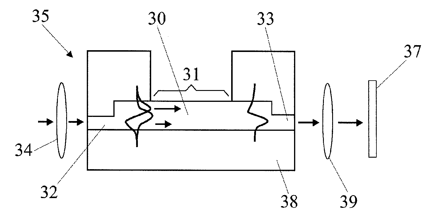
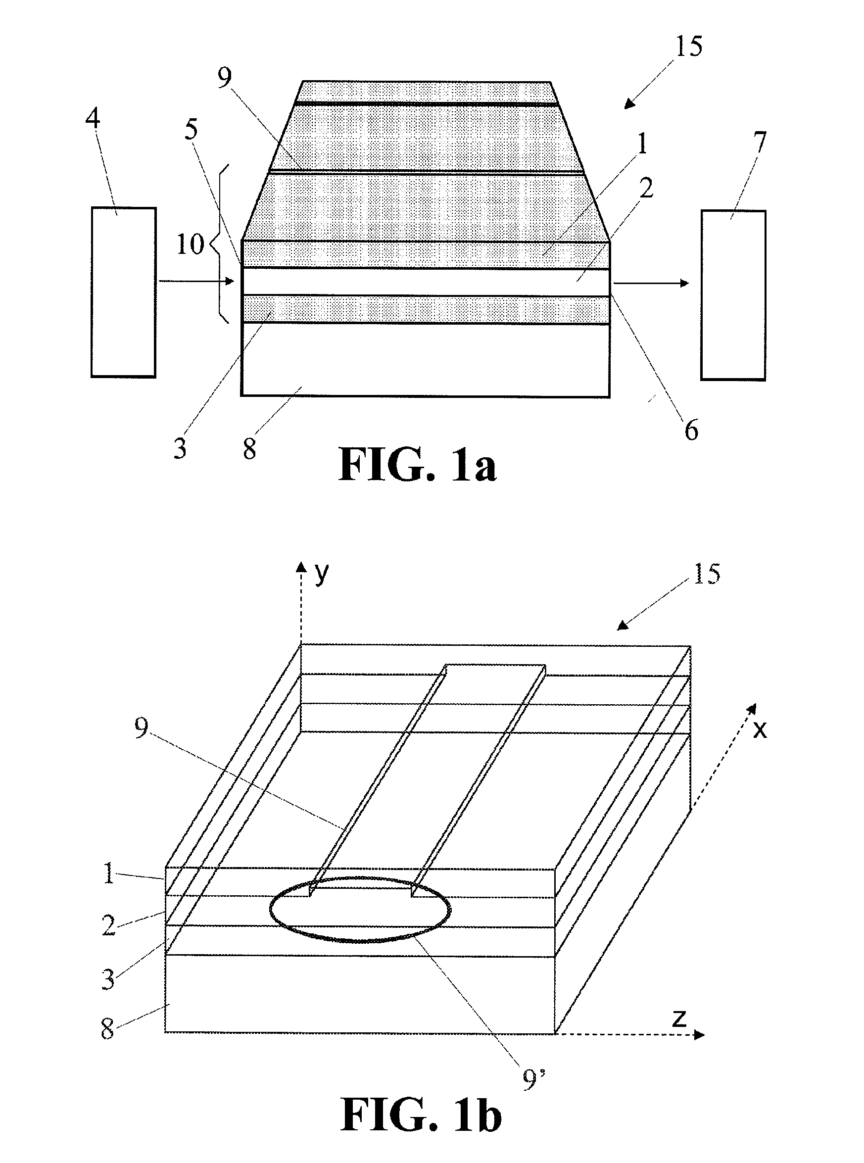
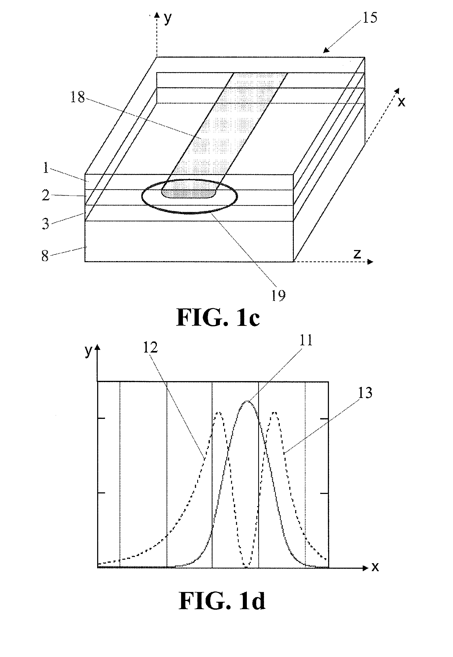
[0043]As illustrated in FIG. 6, a “transverse mode” of a light beam of electromagnetic radiation is a determined intensity pattern of radiation measured along a line formed by a plane (plane 1 or plane YOZ) perpendicular to the propagation direction of light beam and a plane (plane 2 or plane XOY) perpendicular to a waveguide structure and going along the propagation direction. In the context of the present invention, the term “vertical” is to be considered as a synonym of “transverse”.

[0044]As illustrated in FIG. 7, a “lateral mode” of a light beam of electromagnetic radiation is a determined intensity pattern of radiation measured along a line formed by a plane (plane 1 or plane YOZ) perpendicular to the propagation direction of light beam and to a plane (plane 3 or plane XOZ), also perpendicular to the waveguide structure, and going along the propagation direction. In the context of the prese...


PUM


Abstract

Planar optical waveguide interferometer (15, 25, 35, 45) comprising: a substrate (8, 28, 38, 48); a bimodal waveguide (10, 20, 20′, 30, 40) comprising at least one layer (1, 2, 3) deposited on said substrate (8, 28, 38, 48), said bimodal waveguide (10, 20, 20′, 30, 40) being designed for supporting a zero-order and a first-order transverse propagating modes, said transverse propagating modes having different dispersion; a sensor plate (21, 31, 41, 51) located in a selected area of the upper side of said bimodal waveguide (10, 20, 20′, 30, 40), said sensor plate (21, 31, 41, 51) being designed for receiving a chemical, biological or physical stimulus, said stimulus being capable of changing the effective refractive index of said bimodal waveguide (10, 20, 20′, 30, 40). The bimodal waveguide (10, 20, 20′, 30, 40) comprises confining means (9) designed for confining light in lateral direction, the bimodal waveguide (10, 20, 20′, 30, 40) being thus designed for supporting one lateral mode. Chip, sensor and sensing method comprising a planar optical waveguide interferometer are provided.

Description

FIELD OF THE INVENTION[0001]The present invention relates to interferometers and sensors based on optical waveguides, and more particularly, to interferometers and sensors based on bimodal optical waveguides.STATE OF THE ART[0002]Detection of a molecule, e.g. protein, glucose or binding between the molecules is a common issue. The amount of reagent or the concentration of the molecules in the solution may be low and highly sensitive devices are required for the detection of the molecules. The detection can be conducted using various methods and techniques. There exists a variety of nanomechanical and optical devices, such as Mach-Zhender interferometers, Surface Plasmon Resonance, Young interferometers, Fabry-Perot interferometers and slab interferometers. Mach-Zhender and Young interferometers are compact devices based on optical waveguides which were introduced long time ago and have been well studied. Today these techniques are considered to be among the most sensitive ones in th...

Claims


Application Information

Patent Timeline
Patent Type & Authority Applications(United States)
IPC IPC(8): G01B9/02
CPCG01N21/45G01N21/7703G01N2021/458G01N2021/7779G02B2006/12159G02B6/14G02B6/32G02B2006/12107G02B2006/12152G02B6/124
Inventor DOMINGUEZ HORNA, CARLOSZINOVIEV, KIRILLLECHUGA GOMEZ, LAURA MARIA
Owner CONSEJO SUPERIOR DE INVESTIGACIONES CIENTIFICAS (CSIC)
Why Eureka
Try Eureka