Processing Apparatus and Method of Manufacturing Electron Emission Element and Organic EL Display

Inactive Publication Date: 2010-10-28
CANON ANELVA CORP
View PDF4 Cites 10 Cited by
  • Summary
  • Abstract
  • Description
  • Claims
  • Application Information

AI Technical Summary

Benefits of technology

[0040]According to the present invention, even when a mask, which corresponds to the demand for increasing the size of an object to be processed, is used, the highly accurate batch pattern film formation can be realized, and, at the same time, the object to be processed can be prevented from being damaged. Further, it is possible to easily correspond to the demand for increasing the size of the object to be processed.

Problems solved by technology

If the rigidity of the frame is small, the frame itself is deformed by the reaction force, and the tension is relieved, whereby predetermined accuracy cannot be maintained.
Based on the above reasons, in order to realize minute pattern accuracy, the frame of the mask is required to have a high rigidity, which means the increase of the weight of the metal mask.
The multi-piece molding based on the request for the improvement of the processing performance and the increase of the size of an object to be processed itself cause the increase of the size and weight of a mask.
When the size and weight of a mask are increased, a mechanism that aligns the position of the mask with an object to be processed and a mechanism that moves the mask are increased in size, whereby it is difficult for a film formation apparatus to maintain high accuracy.
As the fixing means for a mask and an object to be processed, a magnet is used for fixing a metal mask which is a magnetic body; however, a necessary fixing force is increased as the weight of the mask is increased, whereby damage caused by contact between the mask and the object to be processed and positional deviation caused by impact may occur.
Therefore, when the mask and an object to be processed are in contact with each other, the adherence therebetween decreases, resulting in creases of the mask.
Consequently, when a gap is generated between the contact surfaces between them, a deposition material infiltrates a place other than the opening of the mask, leading to the reduction of the finishing accuracy of the pattern of the mask.

Method used


Image

  • Processing Apparatus and Method of Manufacturing Electron Emission Element and Organic EL Display
  • Processing Apparatus and Method of Manufacturing Electron Emission Element and Organic EL Display
  • Processing Apparatus and Method of Manufacturing Electron Emission Element and Organic EL Display

Examples


Embodiment Construction

[0090]Hereinafter, an embodiment of the present invention will be described with reference to the drawings. In the embodiment, a deposition processing is shown as an example of the processing according to the present invention; however, the processing according to the present invention is not limited to the deposition processing.

[0091]In the present invention, a mask used in a processing apparatus is formed of a magnetic material in a thin film form, and tension is applied to a membranous plane of the mask.

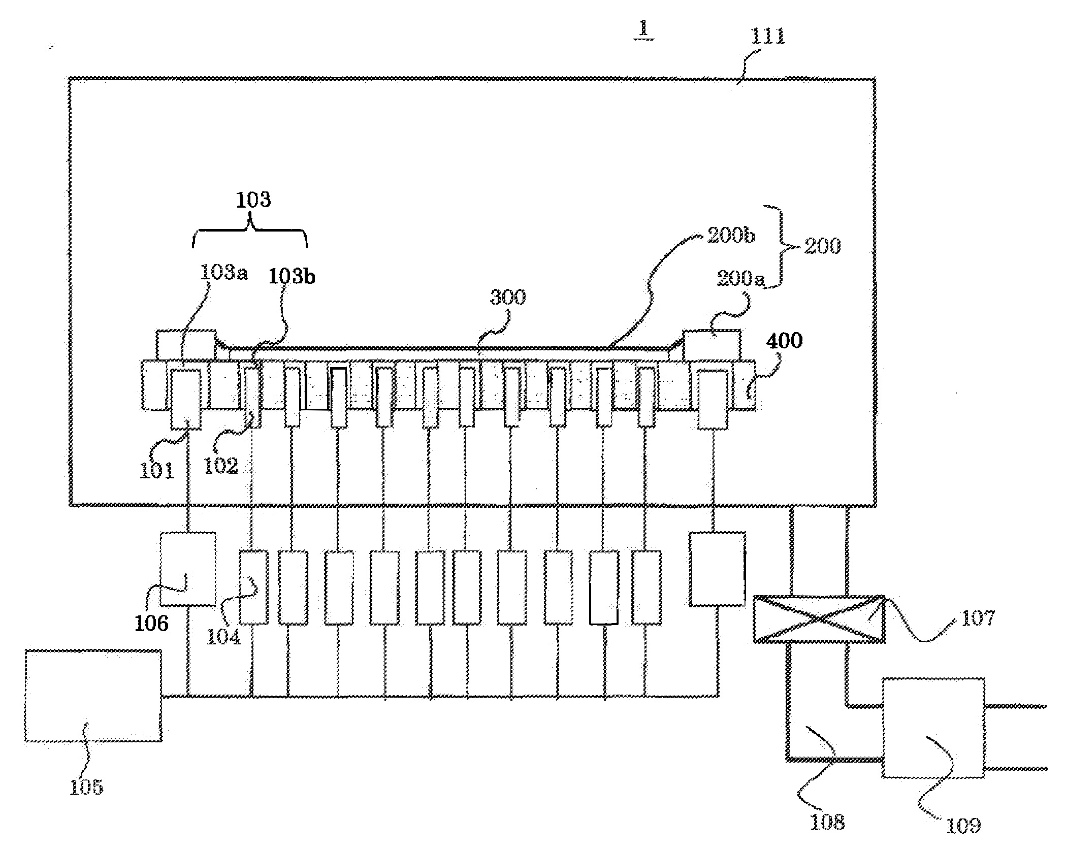
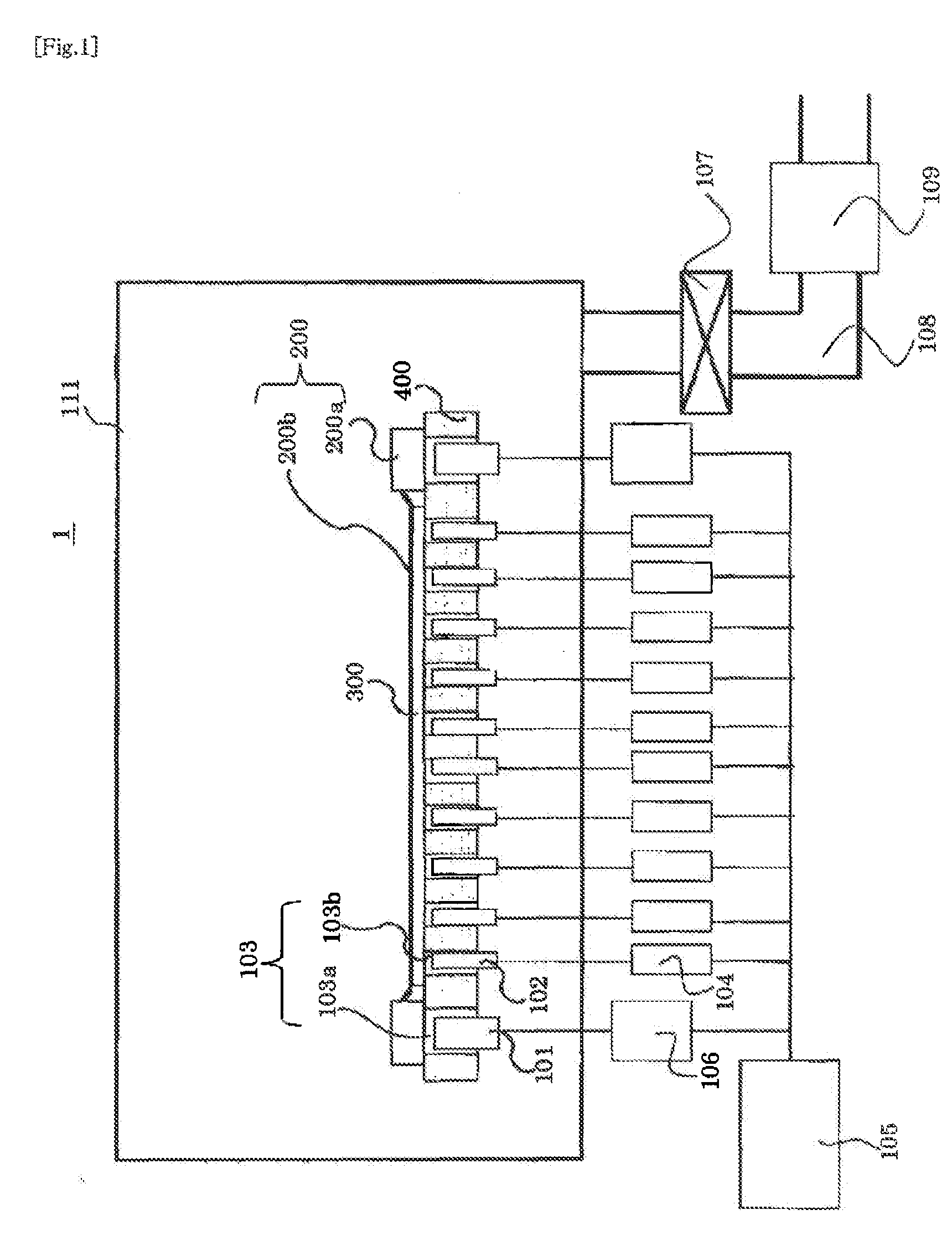
[0092]FIG. 1 is a schematic view of a processing apparatus according to the present invention.

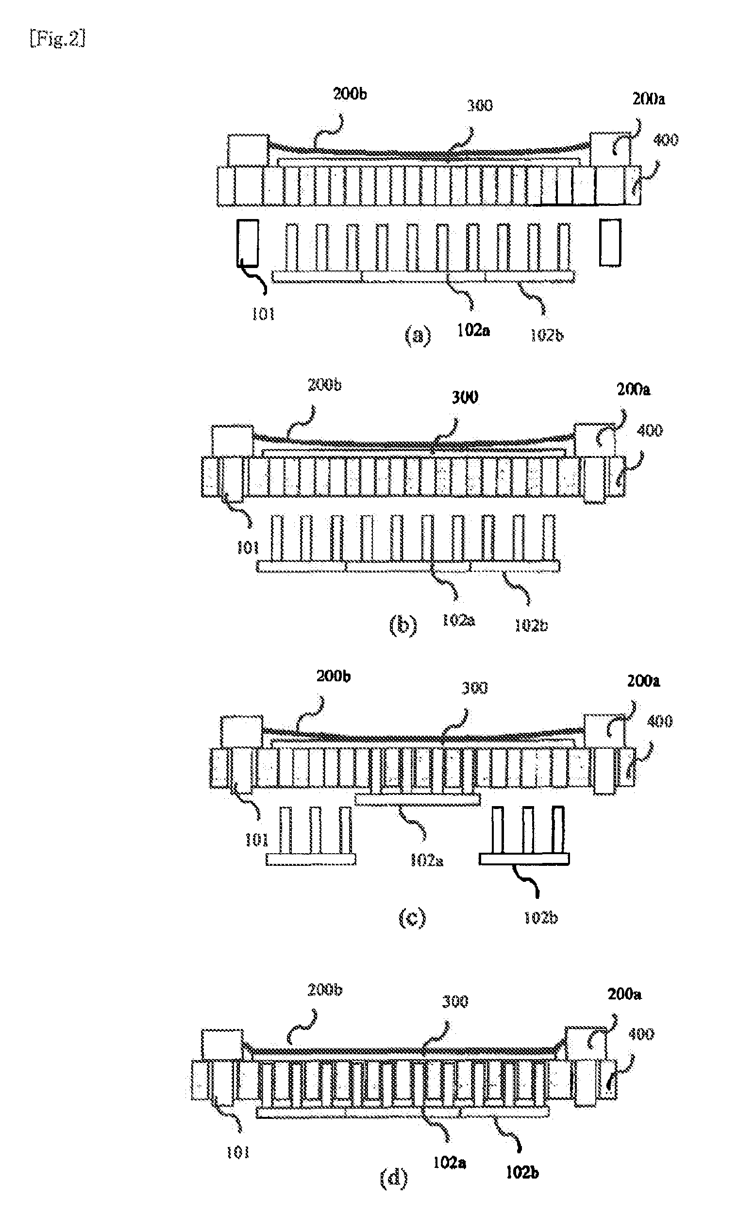
[0093]FIG. 1 shows a state after the mask fixing operation to be described later. A mask fixing device is turned upside down upon deposition, and deposition is performed in such a state that a mask and the processing surface of a substrate are directed downward.

[0094]A processing apparatus 1 includes fixing means (second fixing means) 101 for fixing a mask frame 200a and fixing means (fir...


PUM

PropertyMeasurementUnit
Lengthaaaaaaaaaa
Sizeaaaaaaaaaa
Magnetic forceaaaaaaaaaa

Abstract

Disclosed is a processing apparatus which can realize highly fine batch pattern film formation for a mask, which is significantly increased in weight according to the demand for increasing the size of an object to be processed, whereby leading to a possibility of reduction in the alignment accuracy of a pattern.The processing apparatus 1 which fixes and processes an object to be processed 300 and a mask 200 includes a base 400 on which the object to be processed 300 and the mask 200 are placed. The processing apparatus 1 further includes second fixing means 101 and first fixing means 102. The second fixing means 101 includes a permanent magnet for use in fixing a mask frame 200a of the mask 200 on the base 400. The first fixing means 102 includes a permanent magnet for use in fixing a mask membranous plane 200b of the Mask 200 on the base 400. The second fixing means 101 and the first fixing means 102a, 102b are mechanisms in which each permanent magnet can move the base 400 in a vertical direction.

Description

TECHNICAL FIELD[0001]This invention relates to a processing apparatus, which adheres and fixes a mask to an object subjected to processing such as film formation and forms a desired pattern on the surface of the object other than an area covered by the mask, and a method of manufacturing an electron emission element and an organic EL display using the processing apparatus.BACKGROUND ART[0002]An apparatus for manufacturing an image display apparatus includes, as an example, a glass substrate manufacturing apparatus for a flat panel display typified by an organic electroluminescence element. With regard to such a substrate for a display, in general, a desired pattern is formed on the substrate with desired accuracy, whereby desired functions are imparted to the substrate.[0003]As a pattern formation method, there have been known a vacuum deposition method, a sputtering method, a photolithography method, and a screen printing method. However, at present, a display is required to have a...

Claims


Application Information

Patent Timeline
IPC IPC(8): H01J9/00
CPCC23C14/042C23C14/12H01J9/385H01L51/56H01L27/3211H01L51/0011H01J2209/385H10K59/35H10K71/166H10K71/00H10K71/191
Inventor INOUE, MASATOMATSUI, SHINHIMEJI, TOSHIAKI
Owner CANON ANELVA CORP
Why Eureka
Try Eureka