Microengineered ionisation device
a micro-engineered ionisation and ionisation technology, applied in the field of mass spectrometry, can solve the problems of large system, complex and costly, and limited electrode complexity that can be achieved using such simple mechanical systems
- Summary
- Abstract
- Description
- Claims
- Application Information
AI Technical Summary
Benefits of technology
Problems solved by technology
Method used
Image
Examples
Embodiment Construction
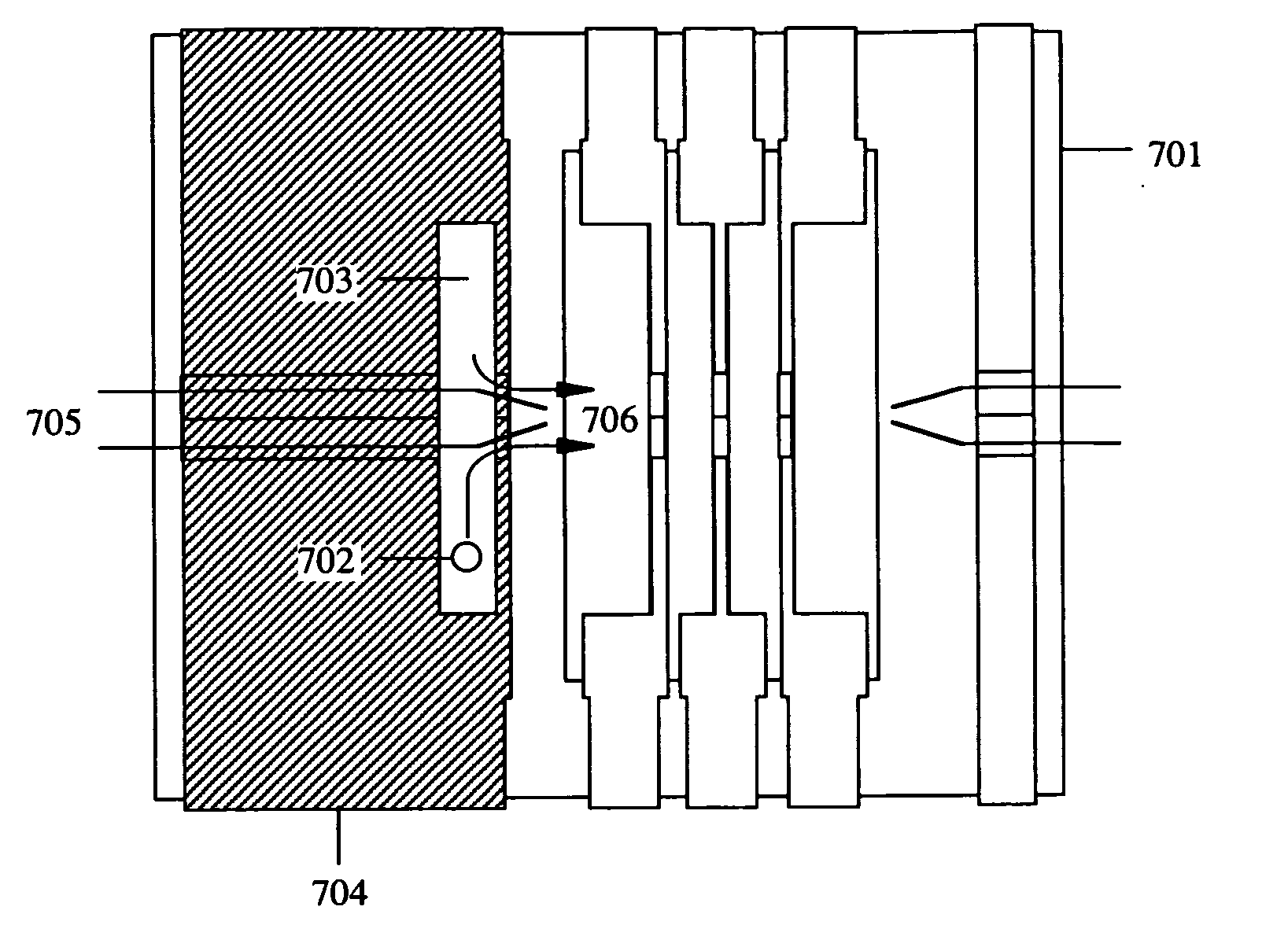
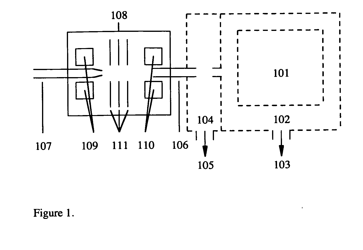
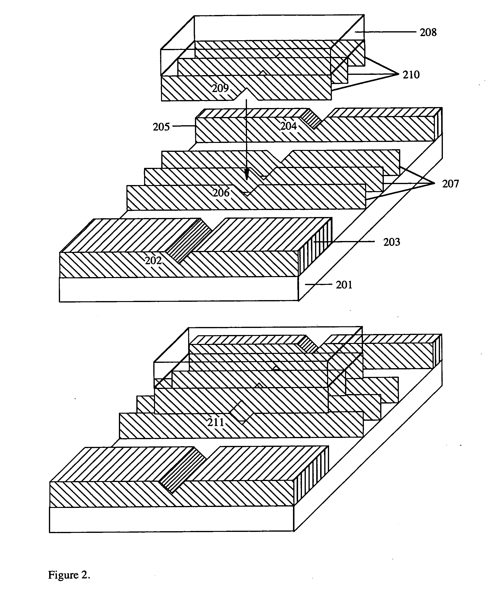
[0037]Features of the invention will now be described with reference to FIGS. 1 to 9, which form part of an earlier application of the present applicant and is currently pending as Patent Application in United Kingdom No. 0519439.4, European Patent Application No. 06117211.0, Patent Application in Canada No. 2552086, Patent Application in Japan No. 2006-197964 and U.S. patent application Ser. No. 11 / 487,735 all of which are as of yet unpublished and are incorporated herein by way of reference. While the present invention shares many features with this earlier application other features are different, the specifics of which will become apparent through a reading of the following.
[0038]The present inventor has realised that the benefit of MEMS or other microengineered structures can be extended to nanospray applications. In MEMS, widely used methods of lithographic patterning, oxidation and metallisation are combined with specialised techniques such as anisotropic wet chemical etching...
PUM
 Abstract
Description
Claims
Application Information
 - R&D
- Intellectual Property
- Life Sciences
- Materials
- Tech Scout
- Unparalleled Data Quality
- Higher Quality Content
- 60% Fewer Hallucinations
Browse by: Latest US Patents, China's latest patents, Technical Efficacy Thesaurus, Application Domain, Technology Topic, Popular Technical Reports.
© 2025 PatSnap. All rights reserved.Legal|Privacy policy|Modern Slavery Act Transparency Statement|Sitemap|About US| Contact US: help@patsnap.com


