

Device and method for signal generation
Patent Information
- Authority / Receiving Office
- US · United States
- Current Assignee / Owner
- NOVATEK MICROELECTRONICS CORP
- Publication Date
- 2010-11-04
- Estimated Expiration
- Not applicable · inactive patent
Smart Images
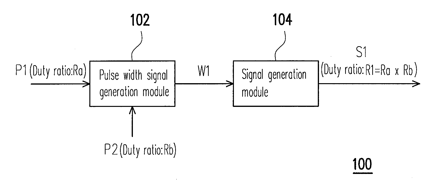
Figure 1 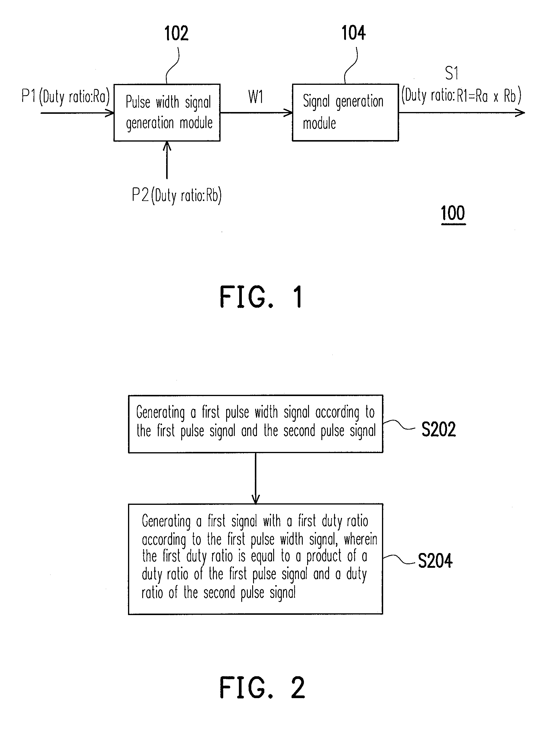
Figure 2 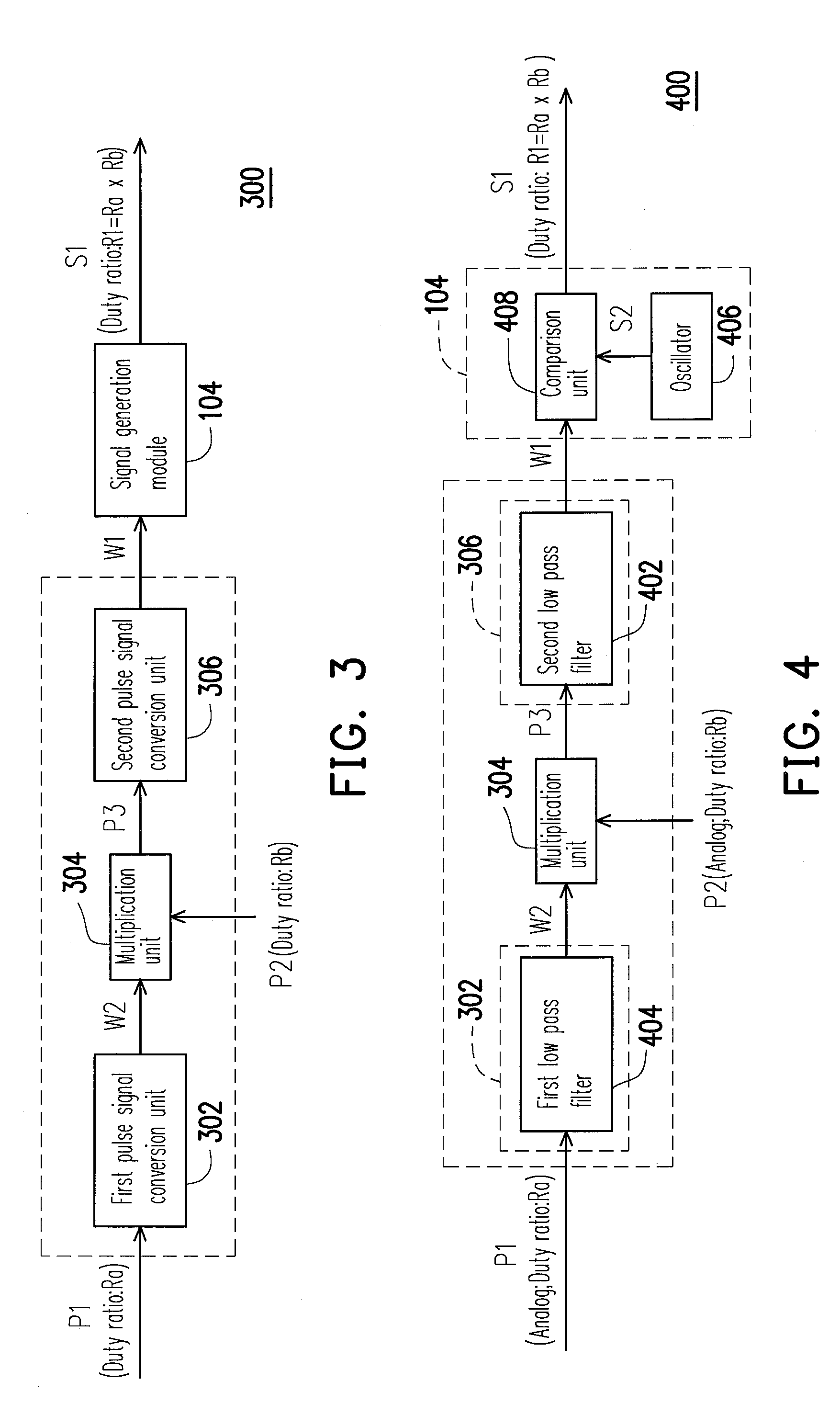
Figure 3
Abstract
Description
CROSS-REFERENCE TO RELATED APPLICATION
[0001] This application claims the priority benefit of Taiwan application serial no. 98114406, filed on Apr. 30, 2009. The entirety of the above-mentioned patent application is hereby incorporated by reference herein and made a part of specification.BACKGROUND OF THE INVENTION
[0002] 1. Field of the Invention
[0003] The present invention is related to a signal generator, and particularly related to a signal generator and a signal generation method thereof for generating an output signal according to information related to duty ratios of a plurality of input signals.
[0004] 2. Description of Related Art
[0005] A periodic signal with a frequency loaded on another periodic signal with a specific frequency is commonly applied in communications and related fields. Wherein, a multiplication of sinusoidal waves may be achieved easily by a mixer, further resulting in frequency addition and subtraction. In addition, a multiplication of amplitudes of two signals m...