Chiplet display with oriented chiplets and busses

a chiplet display and chiplet technology, applied in the field of chiplets, can solve the problems of affecting the operation of the display, the current required to drive an entire row (or column) in the display, and the limited number of rows (or columns) of the passive-matrix drive device, so as to reduce the display area required for the busses, reduce manufacturing steps, and improve the routing of the busses

a chiplet display and chiplet technology, applied in the field of chiplets, can solve the problems of affecting the operation of the display, the current required to drive an entire row (or column) in the display, and the limited number of rows (or columns) of the passive-matrix drive device, so as to reduce the display area required for the busses, reduce manufacturing steps, and improve the routing of the busses

US20100277440A1Active Publication Date: 2010-11-04GLOBAL OLED TECH

Image

  • Chiplet display with oriented chiplets and busses
  • Chiplet display with oriented chiplets and busses
  • Chiplet display with oriented chiplets and busses

Examples


Embodiment Construction

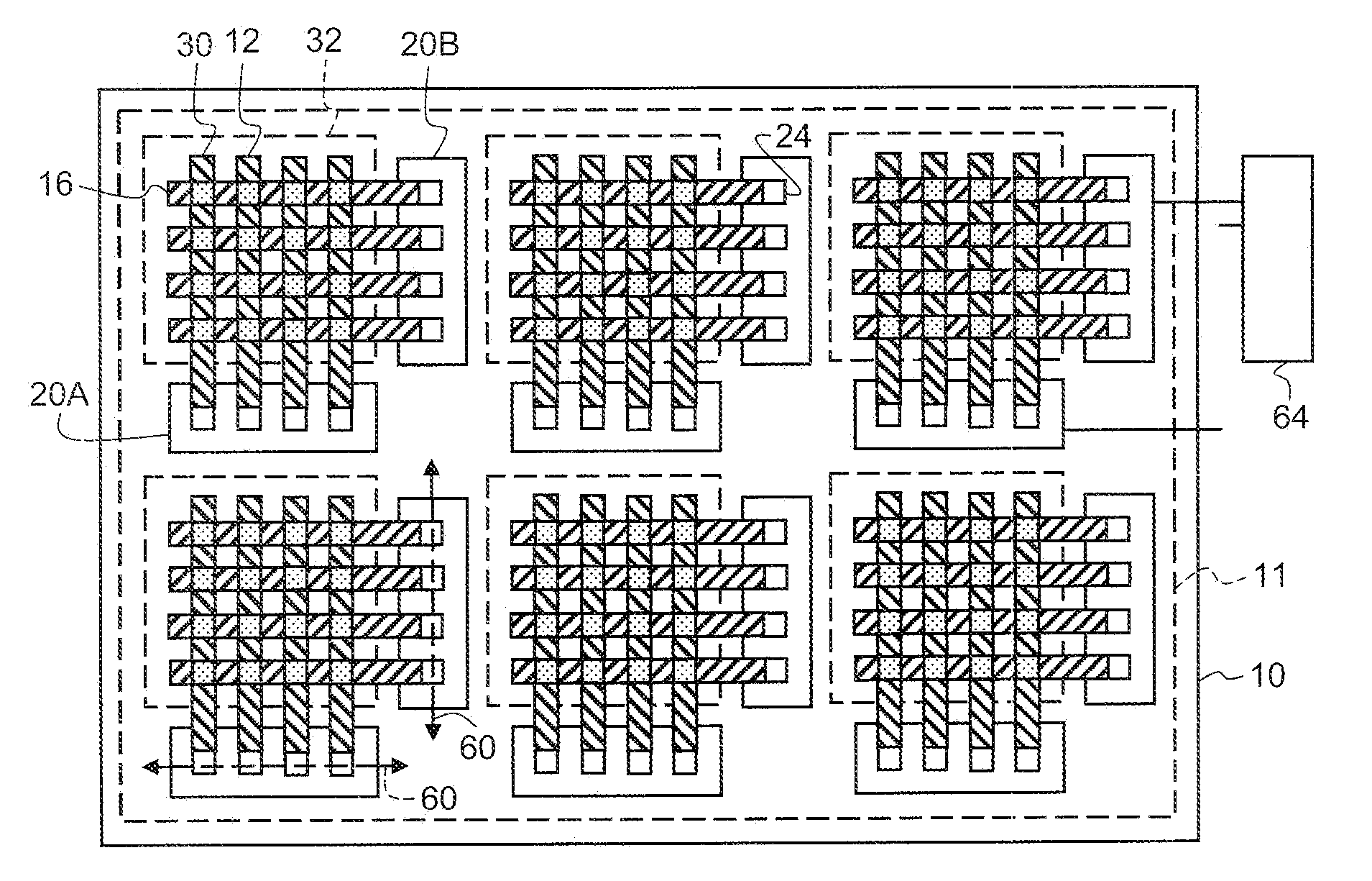
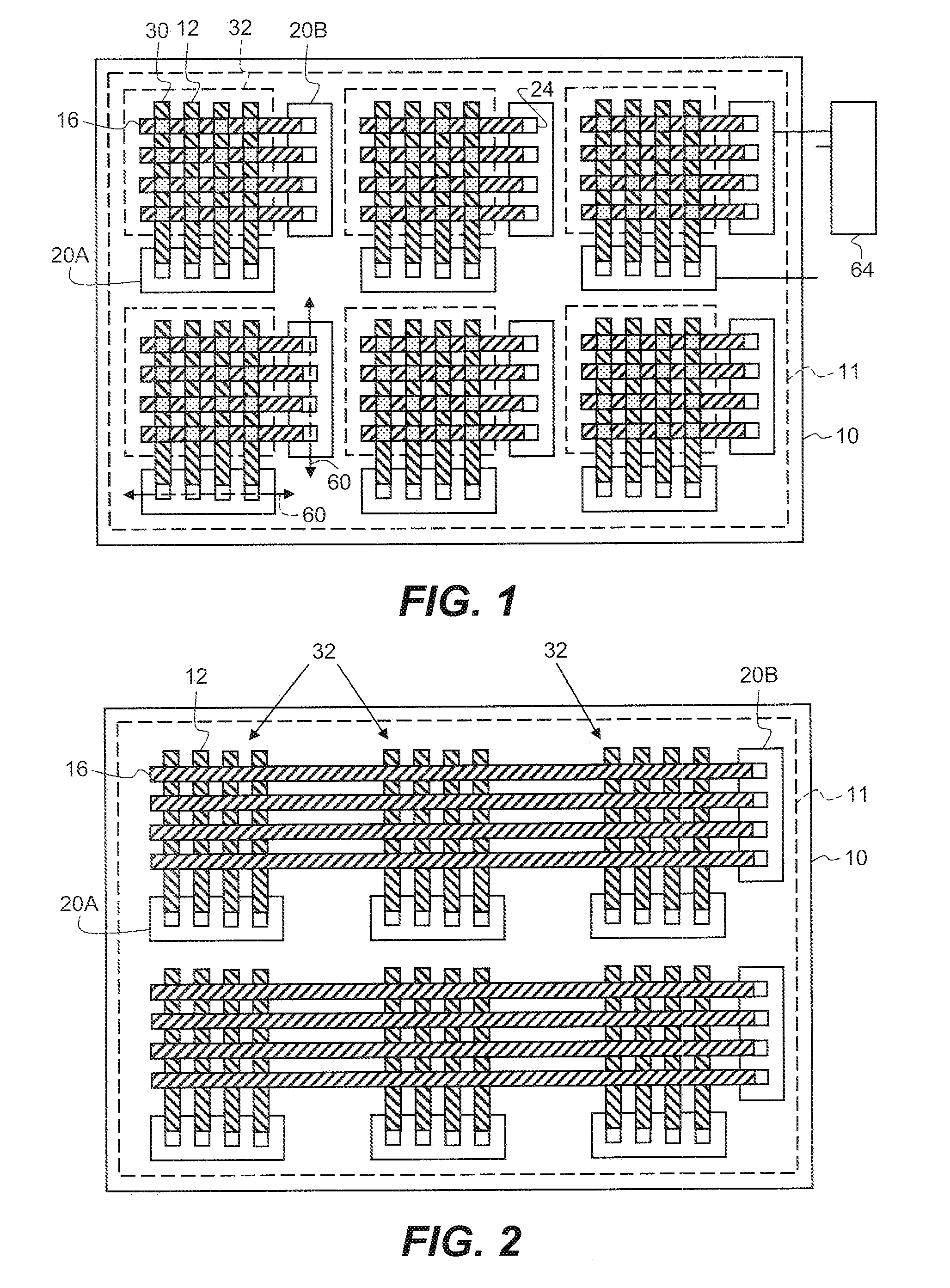
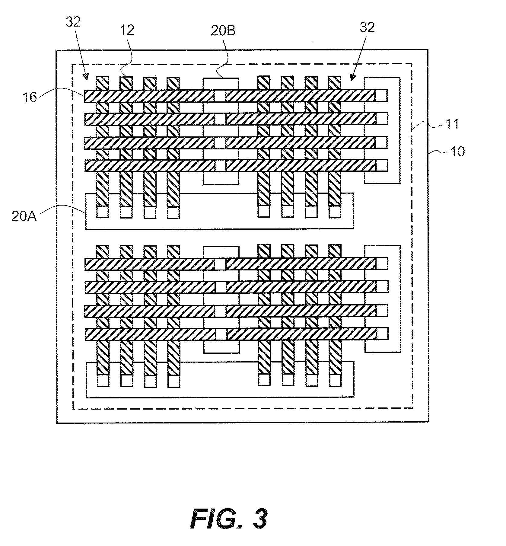
[0032]Referring to FIG. 1, in one embodiment of the present invention, a display device includes a substrate 10 having a display area 11. Two or more column-driver chiplets 20A having connection pads 24 are located over the substrate 10 in the display area 11 and one or more row-driver chiplets 20B having connection pads 24 are also located over the substrate 10 in the display area 11. As shown in FIG. 11, the column- and row-driver chiplets 20A, 20B each have a long axis 60 and a short axis 62. Typically, column and row-driver the chiplets 20A, 20B are rectangular with two opposing sides longer than the other two sides, making a physically high-aspect ratio chiplet with a long dimension and a short dimension. The long axis 60 of the chiplet is in the long dimension; the short axis 62 of the chiplet is in the short dimension. The long axis 60 of each column-driver chiplet 20A is oriented in a row direction. The long axis 60 of each row-driver chiplet 20B is oriented in a column dire...


PUM


Abstract

A display device includes a substrate having a display area; two or more column-driver chiplets having connection pads, each column-driver chiplet having a long axis and located over the substrate in the display area, the long axis of each column-driver chiplet oriented in a row direction; one or more row-driver chiplets having connection pads, each row-driver chiplet having a long axis and located over the substrate in the display area, the long axis of each row-driver chiplet oriented in a column direction different from the row direction; and a first common buss extending over the display area in the row direction connected to a connection pad on each of the row-driver chiplets, the first common buss further including one or more electrically connected first buss portions oriented in the column direction, each first buss portion electrically connected to a connection pad of a respective column-driver chiplet.

Description

CROSS REFERENCE TO RELATED APPLICATIONS[0001]Reference is made to commonly-assigned, co-pending U.S. patent applications: Ser. No. 12 / 371,666 filed Feb. 16, 2009, entitled “Chiplet Display Device with Serial Control” to Cok Ser. No. 12 / 372,132 filed Feb. 17, 2009, entitled “Chiplet Driver Pairs for Two-Dimensional Display” to Cok et al and Ser. No. 12 / 426,986 filed Apr. 21, 2009 entitled “CHIPLET DISPLAY WITH MULTIPLE PASSIVE-MATRIX CONTROLLERS” to Cok, he disclosures of which are incorporated herein.FIELD OF THE INVENTION[0002]The present invention relates to display devices having a substrate with distributed, independent chiplets for controlling a pixel array.BACKGROUND OF THE INVENTION[0003]Flat-panel display devices are widely used in conjunction with computing devices, in portable devices, and for entertainment devices such as televisions. Such displays typically employ a plurality of pixels distributed over a substrate to display images. Each pixel incorporates several, diffe...

Claims


Application Information

Patent Timeline
04 Nov 2010
Publication
US20100277440A1
IPC
G09G5/00
CPC
H01L27/3255; H10K59/129; H10K59/121
Inventors
COK, RONALD S.