Method for Inspecting Overlay Shift Defect during Semiconductor Manufacturing and Apparatus Thereof

Active Publication Date: 2010-11-04
ASML NETHERLANDS BV
View PDF2 Cites 9 Cited by
  • Summary
  • Abstract
  • Description
  • Claims
  • Application Information

AI Technical Summary

Benefits of technology

[0009]In view of the foregoing, one feature of the present invention is to provide a method of inspecting for ov

Problems solved by technology

Overlay shift is a common defect which occurs during the manufacture of semiconductor devices (such as integrated circuits).
Because of overlay shifting, the formed metal lines can fail to be aligned with the underlying contact/via plugs after etching.
This can result in a high contact resistance between the elements.
Such resistance can cause malfunction of the entire device; for example, a disconnected source/drain contact plug with the corresponding bit line can obstruct the op

Method used


Image

  • Method for Inspecting Overlay Shift Defect during Semiconductor Manufacturing and Apparatus Thereof
  • Method for Inspecting Overlay Shift Defect during Semiconductor Manufacturing and Apparatus Thereof
  • Method for Inspecting Overlay Shift Defect during Semiconductor Manufacturing and Apparatus Thereof

Examples


Embodiment Construction

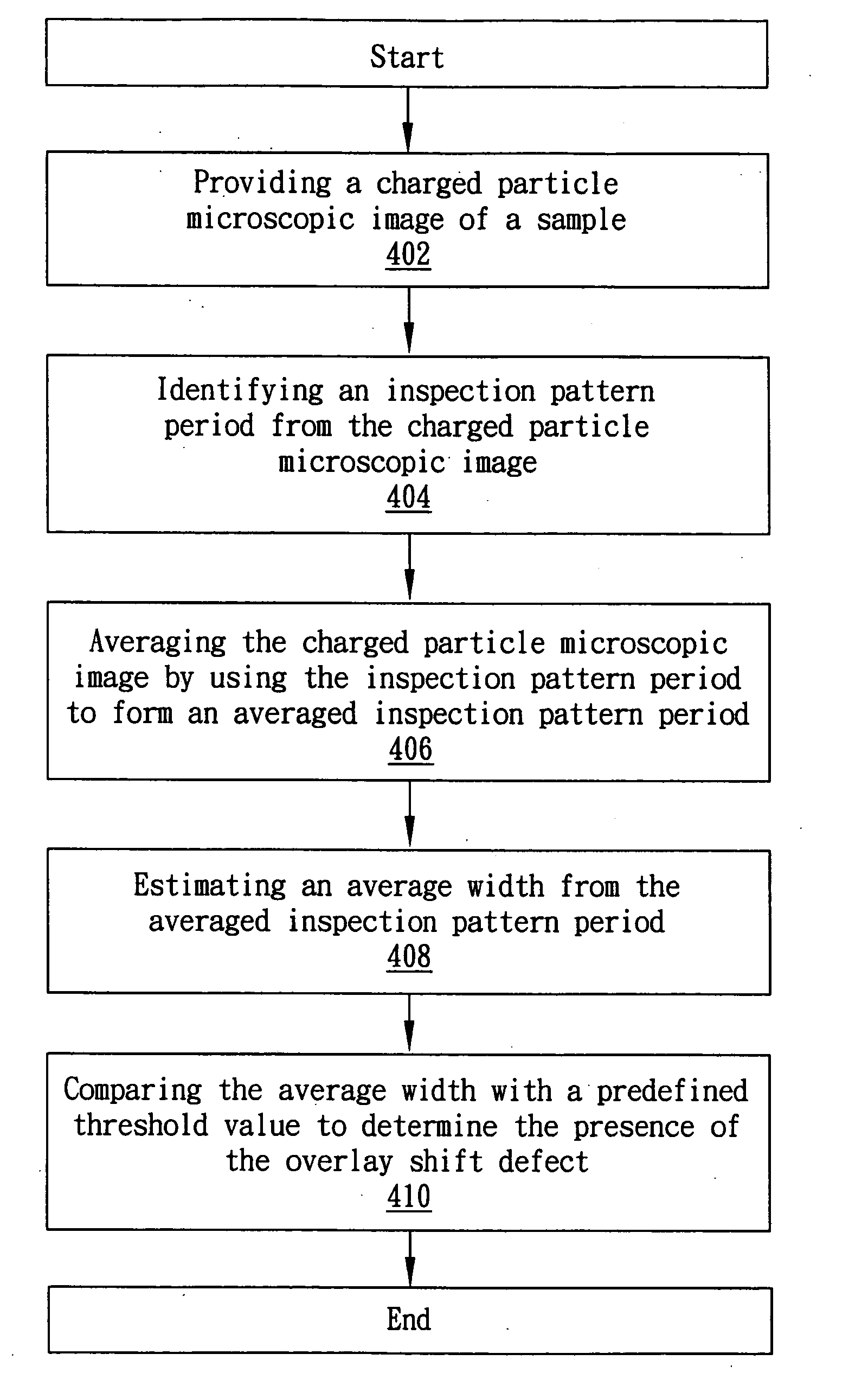
[0021]A detailed description of the present invention will be presented in the following embodiments, which are not intended to limit the scope of the present invention and which can be adapted for other applications. While the drawings are illustrated in detail, it is appreciated that the quantity of the disclosed components may be greater or less than that disclosed, except for occurrences expressly restricting the amount of the components.

[0022]As mentioned earlier, one of the major causes of overlay shift defects is the misalignment of photolithography masks, which are used for forming two successive layers within a semiconductor device. Accordingly, in one embodiment of the present invention, a method of inspecting for misalignments of photolithographic masks from a charged particle microscopic image is disclosed. The charged particle microscopic image may be obtained by a conventional charged particle microscope system such as that described above in conjunction with FIG. 2. F...


PUM


Abstract

A method of inspecting for overlay shift defects during semiconductor manufacturing is disclosed. The method can include the steps of providing a charged particle microscopic image of a sample, identifying an inspection pattern period in the charged particle microscopic image, averaging the charged particle microscopic image by using the inspection pattern period to form an averaged inspection pattern period, estimating an average width from the averaged inspection pattern period, and comparing the average width with a predefined threshold value to determine the presence of an overlay shift defect.

Description

BACKGROUND OF THE INVENTION[0001]1. Field of the Invention[0002]The present invention is related to a method of inspecting for overly shift defects during semiconductor manufacture and apparatus thereof, and more particularly, is related to a method of inspecting for overlay shift between contact / via plugs and metal lines in a semiconductor device using charged particle beam imaging.[0003]2. Description of the Prior Art[0004]Overlay shift is a common defect which occurs during the manufacture of semiconductor devices (such as integrated circuits). One of the major causes of the overlay shift defect stems from misalignment of photolithography masks, which are used for forming two successive layers within a semiconductor device. FIG. 1 is a cross-sectional view showing an overlay shift defect in a semiconductor device. As shown in FIG. 1, overlay shift defects can happen in various layers of a semiconductor device, for example, at the location between a contact plug 104 and a first la...

Claims


Application Information

Patent Timeline
IPC IPC(8): G06K9/00G01N23/00
CPCH01L21/67242G03F7/70633
Inventor XIAO, HONGFANG, WEIJAU, JACK
Owner ASML NETHERLANDS BV
Why Eureka
Try Eureka