DeltaSigma Modulator

a delay compensation and modulator technology, applied in the field of loop delay compensation circuits of modulators, can solve the problems of increasing power consumption and area, large circuit size, and complicated computation, and achieve the effect of low power consumption of the entire circui

Inactive Publication Date: 2010-11-11
SONY CORP
View PDF6 Cites 13 Cited by
  • Summary
  • Abstract
  • Description
  • Claims
  • Application Information

AI Technical Summary

Benefits of technology

[0047]In accordance with the present invention, it is possible to carry out a delay compensation process while preventing the amplitude of a signal appearing at the input node of the quantizer employed i...

Problems solved by technology

In the case of the ΔΣ modulator 2 shown in the block diagram of FIG. 2, however, the filter circuit FLT1 employs a plurality of resistors R and a plurality of S/H circuits so that the ΔΣ modulator 2 has a large power consumption and a large circuit size.
In addition, since the S/H circuit SH1 employs a plurality of resistors R as shown in the block diagram of FIG. 3, the sensitivity to variations of characteristics of devices produced in a...

Method used


Image

  • DeltaSigma Modulator
  • DeltaSigma Modulator
  • DeltaSigma Modulator

Examples


first embodiment

1: First Embodiment

2: Second Embodiment

3: Third Embodiment

1. First Embodiment

First Rough Configuration of the ΔΣ Modulator

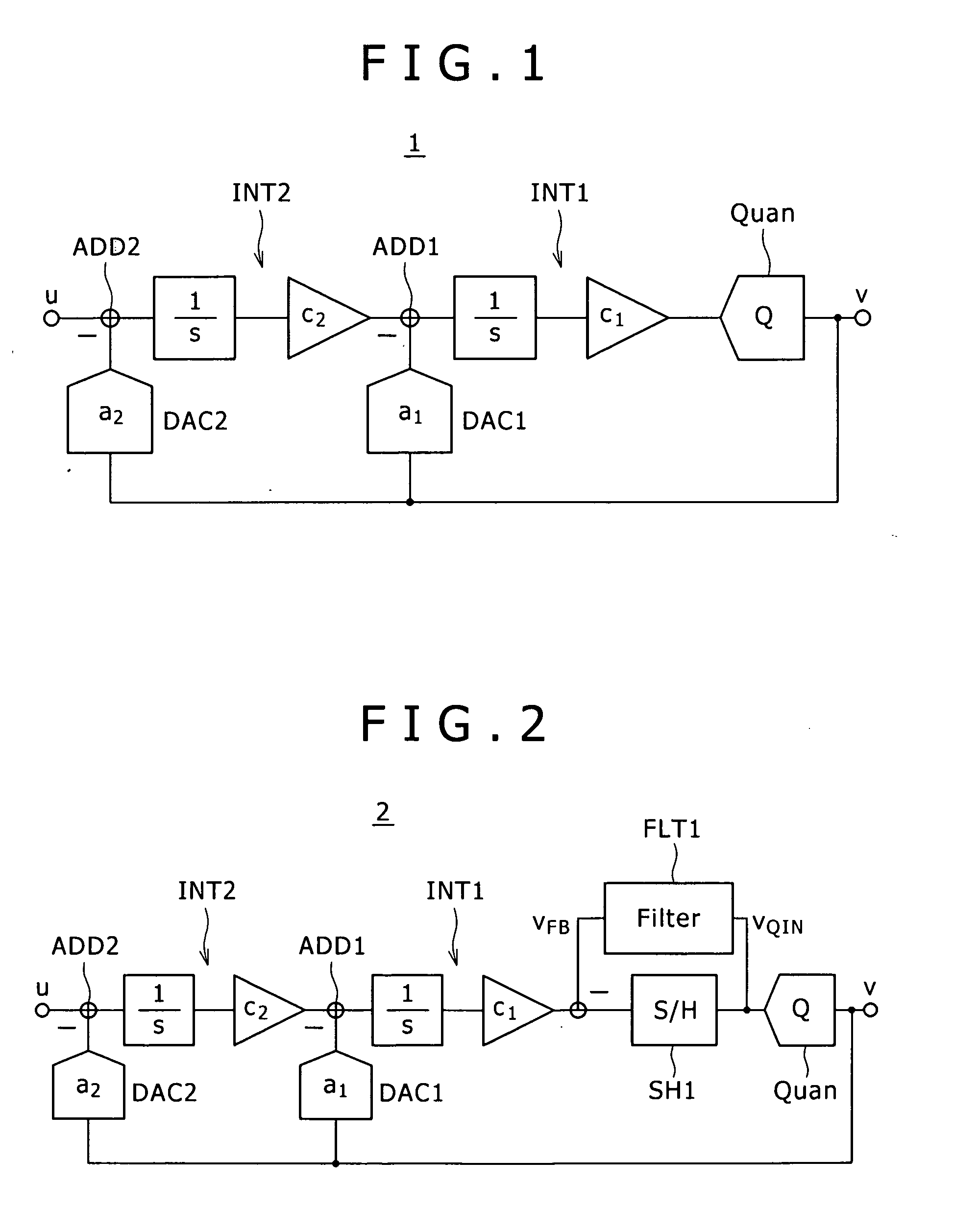
[0066]FIG. 10 is a block diagram showing a rough configuration of a ΔΣ modulator 10 which has a loop delay compensation path according to a first embodiment of the present invention.

[0067]As shown in the block diagram of FIG. 10, the £E modulator 10 employs a first integrator INT11, a second integrator INT12, a quantizer Quan11, a first adder ADD11 serving as a portion of a compensation section and a second adder ADD12.

[0068]The ΔΣ modulator 10 also includes a first DA converter DAC11 and a second DA converter DAC12.

[0069]In the block diagram of FIG. 10, reference notation u denotes an analog input signal supplied to the ΔΣ modulator 10 whereas reference notation Tu denotes an input terminal for receiving the analog input signal u. Reference notation v denotes a digital output signal v generated by the quantizer Quan11 whereas reference notation TV denotes an out...

second embodiment

2. Second Embodiment

Second Rough Configuration of the ΔΣ Modulator

[0131]FIG. 13 is a block diagram showing a rough configuration of a ΔΣ modulator 10B which has a loop delay compensation path according to a second embodiment of the present invention.

[0132]The ΔΣ modulator 10B according to the second embodiment is different from the ΔΣ modulator 10A according to the first embodiment in that the ΔΣ modulator 10B newly employs a third integrator INT13 and a fourth integrator INT14 which are provided between the output side of the second adder ADD12 and the input side of the second integrator INT12.

[0133]In addition, in the case of the ΔΣ modulator 10B according to the second embodiment, a signal output by the fourth integrator INT14 is multiplied by a coefficient b1 in a multiplier section provided on a feed-forward path before being supplied to the first adder ADD11 as a feed-forward signal.

[0134]On top of that, in the case of the ΔΣ modulator 10B according to the second embodiment, a...

third embodiment

3. Third Embodiment

Third Rough Configuration of the ΔΣ Modulator

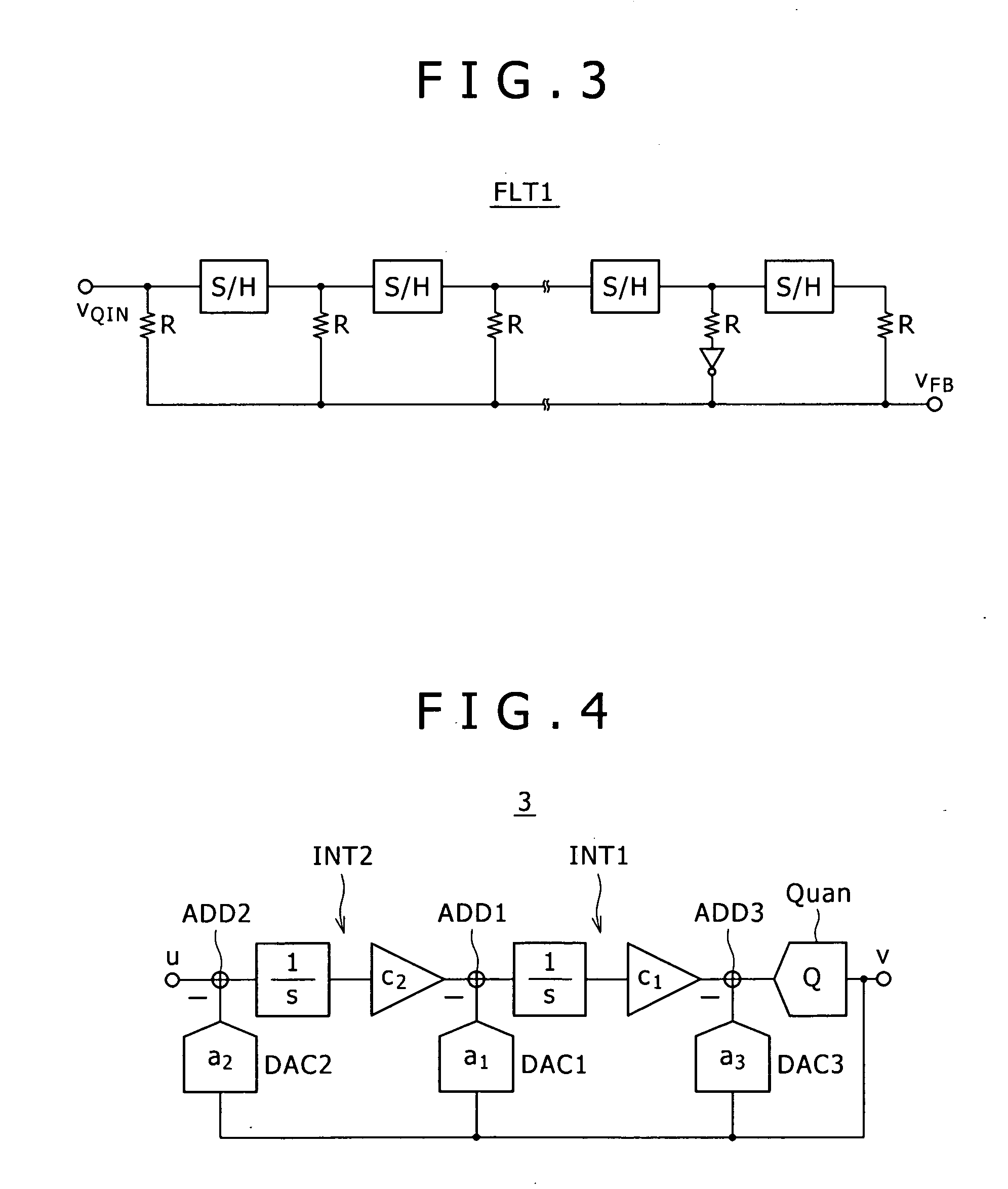
[0159]FIG. 15 is a block diagram showing a rough configuration of a ΔΣ modulator 10D which has a loop delay compensation path according to a third embodiment of the present invention.

[0160]The ΔΣ modulator 10D shown in the block diagram of FIG. 15 to serve as a ΔΣ modulator according to the third embodiment is designed to operate as a second-order 1-bit feedback complex ΔΣ modulator.

[0161]By setting the feedback gain of the first DA converter DAC11D employed in the ΔΣ modulator 10D at [a1+k(s−jω)], it is possible to realize a feedback path which has a frequency-independent part for delay compensation.

[0162]In addition, a third adder ADD13 is provided on the output side of the first integrator INT11D and a signal output by the second integrator INT12D is multiplied by a coefficient b1 in a multiplier section provided on a feed-forward path before being supplied to the third adder ADD13 as a feed-forward signal.

Third Conc...


PUM


Abstract

Disclosed herein is a ΔΣ modulator including: at least one integrator; a quantizer for quantizing a signal output by the integrator and outputting the quantized signal as a digital signal; and a compensation section configured to compensate the ΔΣ modulator for a non-ideal characteristic caused by an internal loop delay, wherein the compensation section is a feedback path formed to start at the output node of the quantizer and end at the input node of the integrator immediately preceding the quantizer, and the feedback path formed to start at the output node of the quantizer and end at the input node of the integrator realizes a frequency-independent part in combination with the integrator and an internal DA converter which adopts the NRZ technique to suppress the signal amplitude at the quantizer input.

Description

BACKGROUND OF THE INVENTION[0001]1. Field of the Invention[0002]In general, the present invention relates to a continuous-time-system ΔΣ modulator applied to audio-electronic and medical-treatment / measurement apparatus and the like in addition to radio-communication receivers which serve as main applications. More particularly, the present invention relates to a loop delay compensation circuit of the ΔΣ modulator.[0003]2. Description or the Related Art[0004]FIG. 1 is a block diagram showing an ordinary second-order low-pass ΔΣ modulator 1 of the continuous time system.[0005]The ΔΣ modulator 1 shown in the block diagram of FIG. 1 is configured to employ integrators INT1 and INT2, a quantizer Quan, adders ADD1 and ADD2 as well as DA (Digital-to-Analog) converters DAC1 and DAC2.[0006]In the block diagram of FIG. 1, reference notation u denotes an analog input signal whereas reference notation v denotes a digital output signal. Reference notations a1 and a2 denote the feedback gains of ...

Claims


Application Information

Patent Timeline
IPC IPC(8): H03M3/00
CPCH03M3/37H03M3/454H03M3/43
Inventor NIWA, ATSUMIMATSUMOTO, TOMOHIROMOUE, TAKASHI
Owner SONY CORP
Why Eureka
Try Eureka