Manufacturing method of a packaging structure of electronic components

a manufacturing method and electronic component technology, applied in the direction of semiconductor devices, semiconductor/solid-state device details, small component housings, etc., can solve the problems of emi only being minimized, affecting the overall performance of the circuit, and unable to completely eliminate emi, so as to reduce the complexity of manufacturing an electronic module that is anti-emi and reduce the cost , the effect of high complicacy

Inactive Publication Date: 2010-11-11
ACSIP TECH
View PDF4 Cites 26 Cited by
  • Summary
  • Abstract
  • Description
  • Claims
  • Application Information

AI Technical Summary

Benefits of technology

[0009]By providing the manufacturing method of a packaging structure of electronic components according to the present invention, the manufacturing of an anti-EMI electronic module can be less complicated and make better the circuit design in miniaturization, high complicacy and reduced cost.

Problems solved by technology

In circuit design, leads, circuit boards, and / or various electronic components can generate electromagnetic waves which may affect the overall performance of the circuit.
In practice, the EMI is unable to be completely eliminated.
Actually, problems caused by the EMI can only be minimized by excellent circuit design and route design.
Amid the trend of miniaturization, high frequency, and higher density of distribution in electronic design, the problems of EMI can only become more troublesome and hard to be handled.
However, the application of the aforesaid three modules in a single tiny substrate or product can only make the EMI problem (mainly by interacting) more severely.
It can be foreseen that, in the modern communication product, interacting EMI problem among built-in modules inside an individual system become a real issue.
It is easy to see that the conventional metal housing, which is applied to shield a system or an equipment, is no more relevant to solve the interacting EMI problem inside a single system or module, which provides only extremely limited and irregular space for anti-EMI construction.
Besides, it is also technically difficult and also expensive to manufacture tiny metal housings for individual elements in the same electronic product so as to reduce internal EMIs from those different wireless modules.

Method used


Image

  • Manufacturing method of a packaging structure of electronic components
  • Manufacturing method of a packaging structure of electronic components
  • Manufacturing method of a packaging structure of electronic components

Examples


Embodiment Construction

[0018]The present invention relates to a manufacturing method of a packaging structure of electronic components, and particularly relates to the manufacturing method that can provide a packaging structure having an effect on blocking the EMI. The following embodiments are included to provide a further understanding to the present invention. Persons having ordinary skill in the art should know the embodiments are for better explanation of the present invention and are not for limiting the present invention. Preferable embodiments of the present invention are as below.

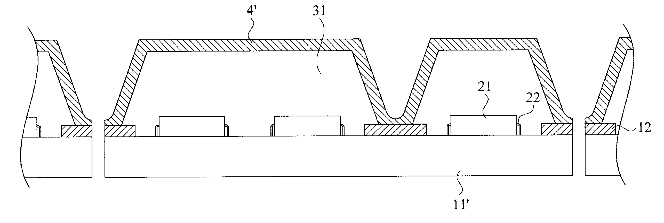
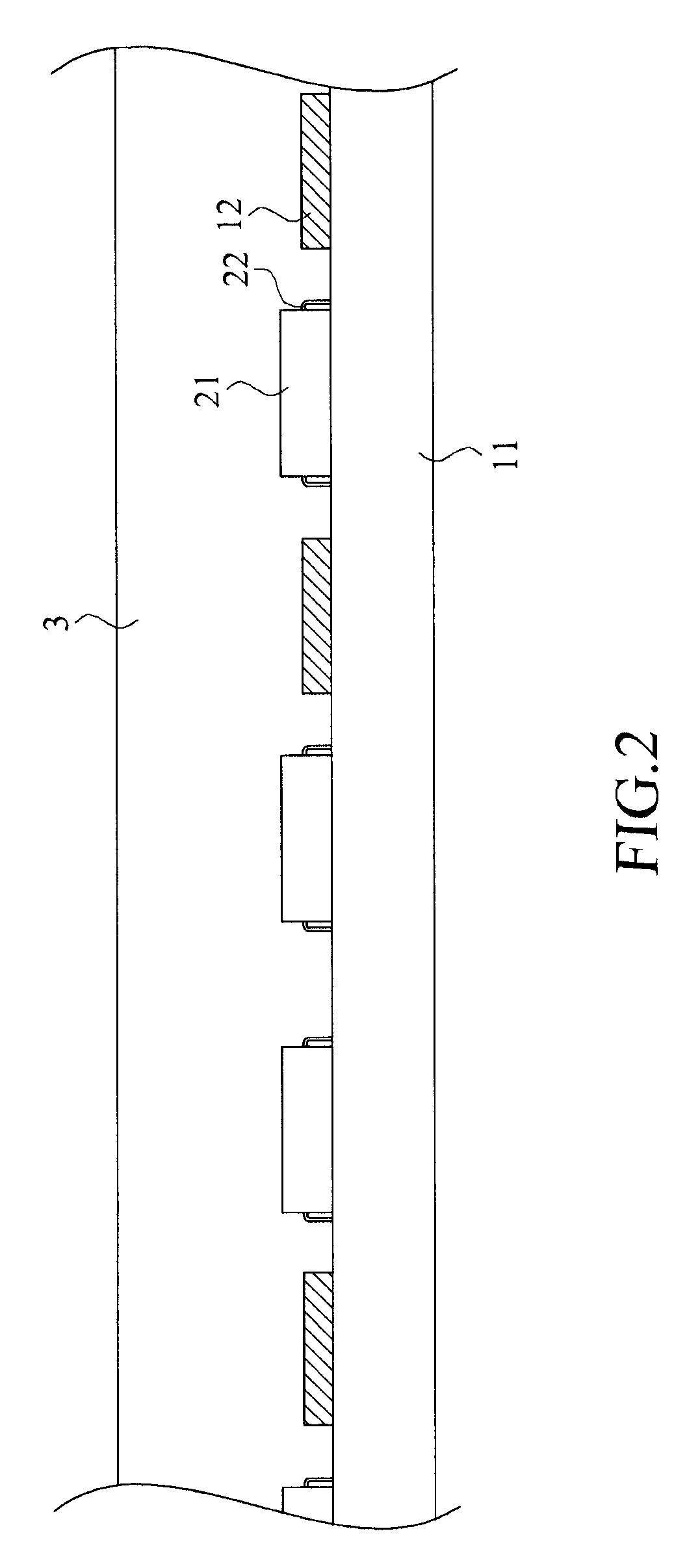
[0019]Referring to FIG. 1, a schematic drawing of a substrate 11 having thereon a plurality of electronic components 21 to be packaged according to a preferred embodiment of the present invention is shown. In the present invention, a manufacturing method of a packaging structure of electronic components 21 includes the steps of: (a) providing a substrate 11 having a plurality of electronic components 21 mounted thereon; ...


PUM


Abstract

A manufacturing method of a packaging structure of electronic components includes the steps of: providing a substrate including a plurality of electronic components; covering the electronic components disposed on the substrate with a molding body; forming a plurality of pre-cut grooves on the molding body so as to define a plurality of molding units on the molding body; forming an electromagnet barrier layer covering the molding units on the molding units and the pre-cut grooves; and cutting along at least one of the pre-cut grooves deeply down to break the substrate so as to form separately a plurality of packaging structures of the electronic components.

Description

FIELD OF THE INVENTION[0001]The present invention relates to a manufacturing method of a packaging structure of electronic components, and particularly relates to a manufacturing method of a packaging structure of electronic components that is able to block the electromagnetic interference (EMI).BACKGROUND OF THE INVENTION[0002]In circuit design, leads, circuit boards, and / or various electronic components can generate electromagnetic waves which may affect the overall performance of the circuit. Such a phenomenon is the so-called electromagnetic interference (EMI). In practice, the EMI is unable to be completely eliminated. Actually, problems caused by the EMI can only be minimized by excellent circuit design and route design.[0003]In related art, it is common to shield an electronic component by a metal housing which forms a conducting barrier for blocking possible electromagnetic waves so as to reduce the effect of the EMI.[0004]Amid the trend of miniaturization, high frequency, a...

Claims


Application Information

Patent Timeline
Patent Type & Authority Applications(United States)
IPC IPC(8): H01L21/82
CPCH01L21/561H01L23/3121H01L23/552H01L25/165H01L2924/1815H05K5/0091H05K9/0037H01L24/97H01L2924/3025
Inventor CHEN, HUAI-TE
Owner ACSIP TECH
Why Eureka
Try Eureka