Method of fabricating semiconductor transistor devices with asymmetric extension and/or halo implants

a technology of semiconductor transistors and halo implants, which is applied in the manufacture of transistors, semiconductor/solid-state devices, electric devices, etc., can solve the problems of asymmetric extension and/or halo implants being difficult (if not impossible) to create, and the photolithography tools that exist are not suitable for modern small-scale process node technology

Inactive Publication Date: 2010-11-11
ALSEPHINA INNOVATIONS INC
View PDF2 Cites 12 Cited by
  • Summary
  • Abstract
  • Description
  • Claims
  • Application Information

AI Technical Summary

Benefits of technology

[0004]A method of fabricating semiconductor devices is provided. The method involves the fabrication of a device structure comprising a semiconductor material and a plurality of gate structures formed overlying the semiconductor material. The method also creates light dose extension implants in the semiconductor material, using the plurality of gate structures as a first implantation mask, by bombarding the device structure with ions at a non-tilted angle relative to an exposed surface of the semiconductor material. Then, the method forms a patterned mask overlying ...

Problems solved by technology

Unfortunately, existing photolithography tools are not suitable for modern small-scale process node technology, e.g., 32 nm or 22 nm nodes, which can be used to create gate structures having a pitch of only 130 nm or less.
Asymmetric extension and/or halo implants are very difficult (if not impo...

Method used


Image

  • Method of fabricating semiconductor transistor devices with asymmetric extension and/or halo implants
  • Method of fabricating semiconductor transistor devices with asymmetric extension and/or halo implants
  • Method of fabricating semiconductor transistor devices with asymmetric extension and/or halo implants

Examples


Embodiment Construction

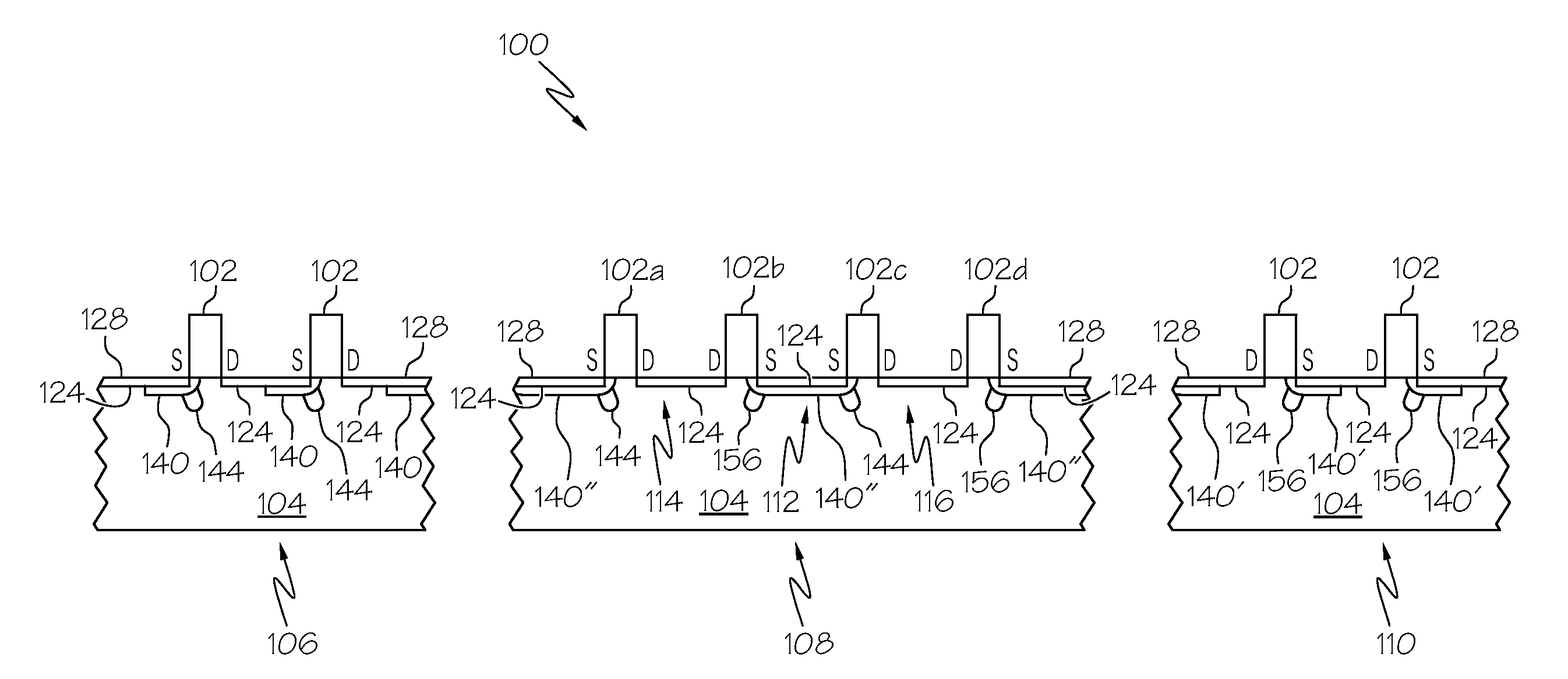
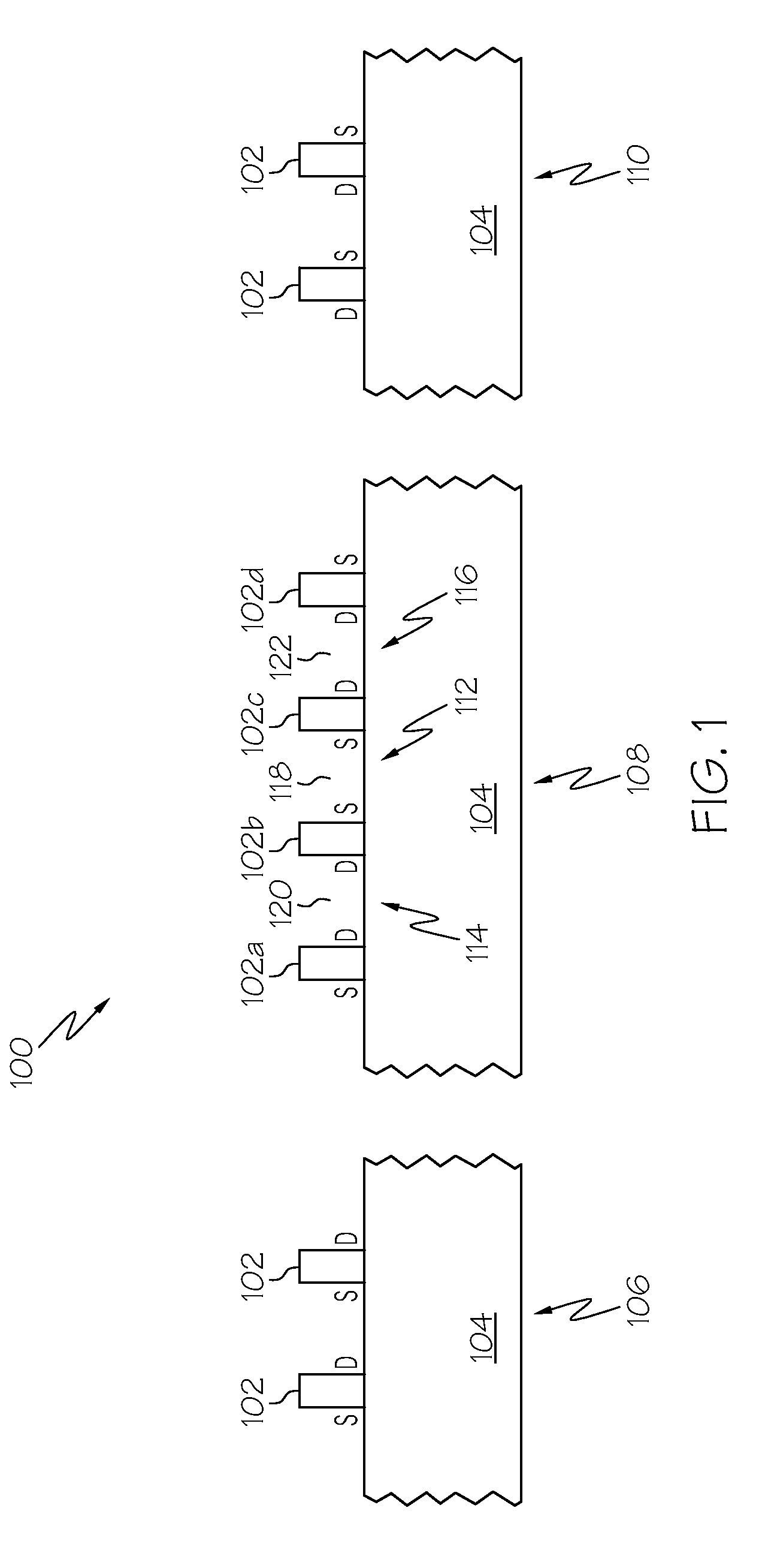
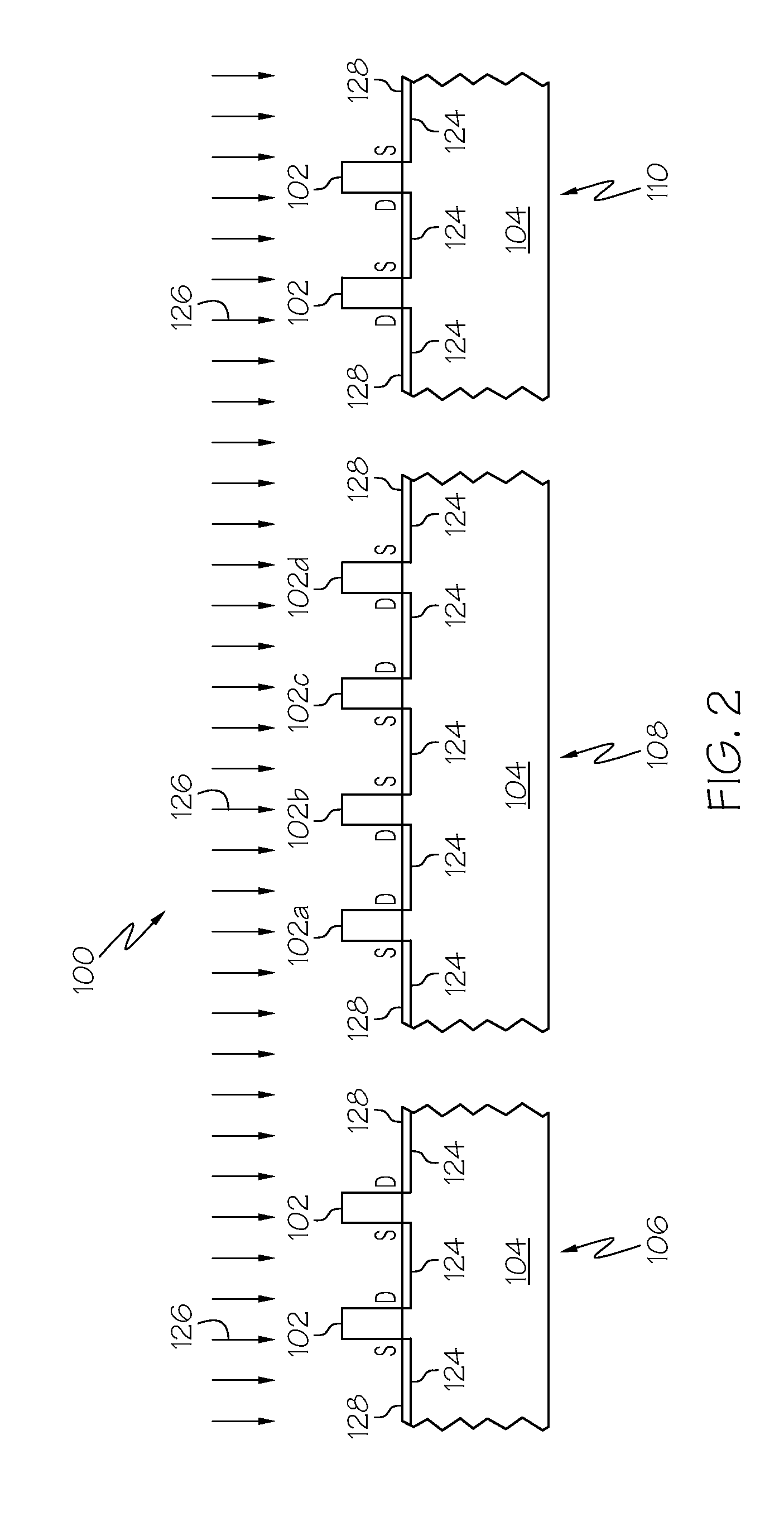
[0011]The following detailed description is merely illustrative in nature and is not intended to limit the embodiments of the subject matter or the application and uses of such embodiments. As used herein, the word “exemplary” means “serving as an example, instance, or illustration.” Any implementation described herein as exemplary is not necessarily to be construed as preferred or advantageous over other implementations. Furthermore, there is no intention to be bound by any expressed or implied theory presented in the preceding technical field, background, brief summary or the following detailed description.

[0012]For the sake of brevity, conventional techniques related to semiconductor device fabrication may not be described in detail herein. Moreover, the various tasks and process steps described herein may be incorporated into a more comprehensive procedure or process having additional steps or functionality not described in detail herein. In particular, various steps in the manu...


PUM


Abstract

A method of fabricating semiconductor devices begins by providing or fabricating a device structure that includes a semiconductor material and a plurality of gate structures formed overlying the semiconductor material. The method continues by creating light dose extension implants in the semiconductor material by bombarding the device structure with ions at a non-tilted angle relative to an exposed surface of the semiconductor material. During this step, the plurality of gate structures are used as a first implantation mask. The method continues by forming a patterned mask overlying the semiconductor material, the patterned mask being arranged to protect shared drain regions of the semiconductor material and to leave shared source regions of the semiconductor material substantially exposed. Thereafter, the method creates heavy dose extension implants and/or halo implants in the semiconductor material by bombarding the device structure with ions at a tilted angle relative to the exposed surface of the semiconductor material, and toward the plurality of gate structures. During this step, the plurality of gate structures and the patterned mask are used as a second implantation mask.

Description

TECHNICAL FIELD[0001]The subject matter described herein relates generally to the fabrication of semiconductor devices. More particularly, the subject matter relates to the fabrication of asymmetric transistor devices.BACKGROUND[0002]The prior art is replete with different techniques and processes for fabricating semiconductor devices such as metal oxide semiconductor (MOS) transistors. In accordance with typical fabrication techniques, a MOS transistor is formed by creating a device structure on a semiconductor substrate, where the device structure includes a gate stack formed on a layer of semiconductor material, and source and drain regions formed in the semiconductor material to define a channel region under the gate stack. Some transistor devices are intentionally fabricated with asymmetric characteristics to improve their performance. For example, a known fabrication process results in asymmetric extension and / or halo implants in the source and drain regions. In particular, th...

Claims


Application Information

Patent Timeline
IPC IPC(8): H01L21/265H01L21/266
CPCH01L21/26586H01L29/1083H01L29/7835H01L29/6659H01L29/66659H01L29/66537
Inventor SHI, ZHONGHAIZHOU, JINGRONG
Owner ALSEPHINA INNOVATIONS INC
Why Eureka
Try Eureka