3D integration structure and method using bonded metal planes

a technology of bonded metal planes and integrated circuits, applied in semiconductor devices, semiconductor/solid-state device details, electrical apparatus, etc., can solve the problems of minimum size needed to make these components, physical limits of the density that can be achieved in two dimensions, and the requirement of more complex designs

Active Publication Date: 2010-11-18
TESSERA INC
View PDF5 Cites 128 Cited by
  • Summary
  • Abstract
  • Description
  • Claims
  • Application Information

AI Technical Summary

Benefits of technology

[0031]a second semiconductor structure comprising a second semiconductor wafer, a front end of the line (FEOL) wiring on the second semiconductor wafer, a back end of the line (BEOL) wiring on the FEOL wiring, an i...

Problems solved by technology

Although dramatic improvements in lithography have resulted in considerable improvements in 2D integrated circuit formation, there are physical limits to the density that can be achieved in two dimensions.
One of these limits is the minimum size needed to make these components.
Also, when more devices are put into one chip...

Method used


Image

  • 3D integration structure and method using bonded metal planes
  • 3D integration structure and method using bonded metal planes
  • 3D integration structure and method using bonded metal planes

Examples


Embodiment Construction

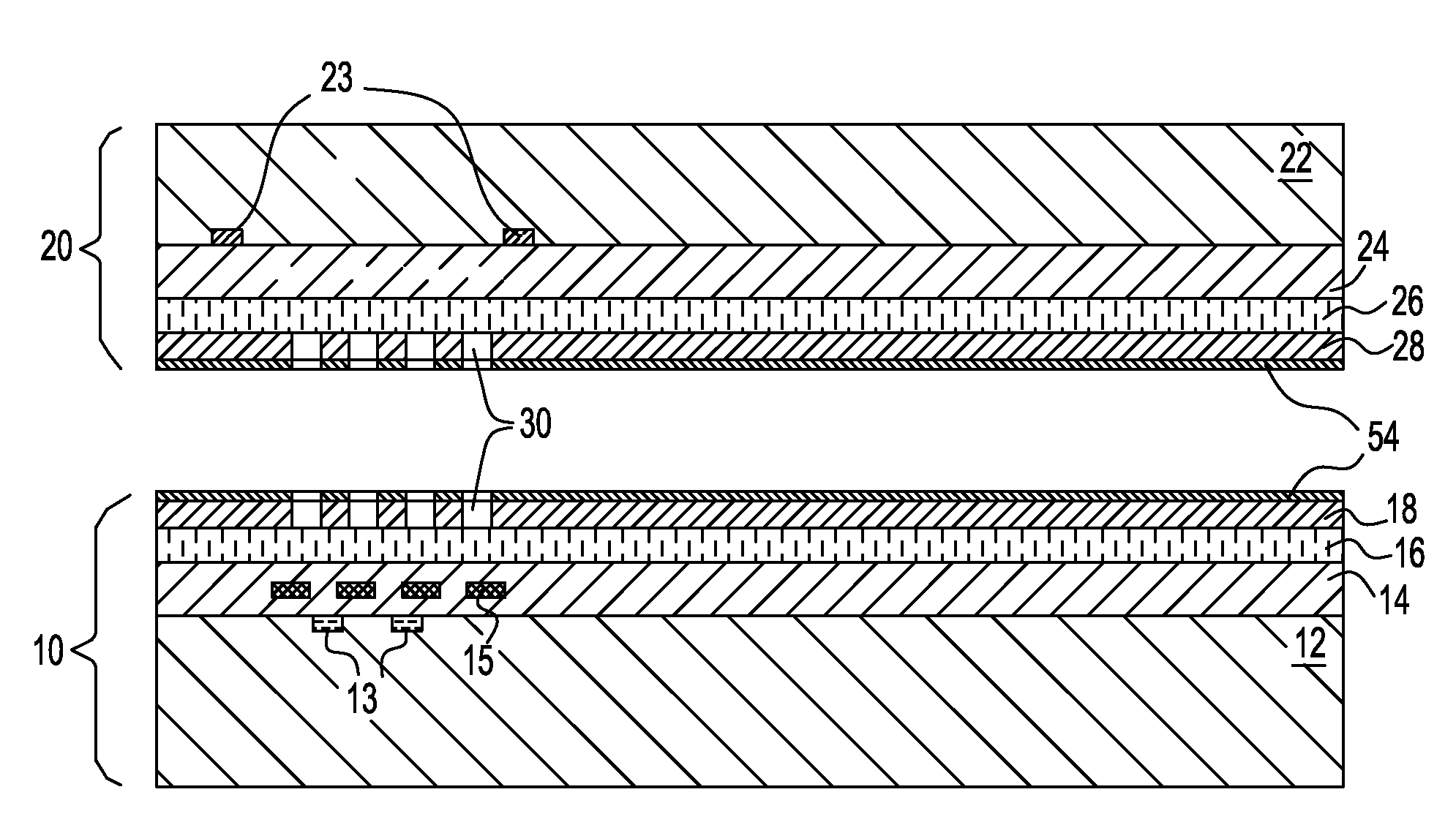
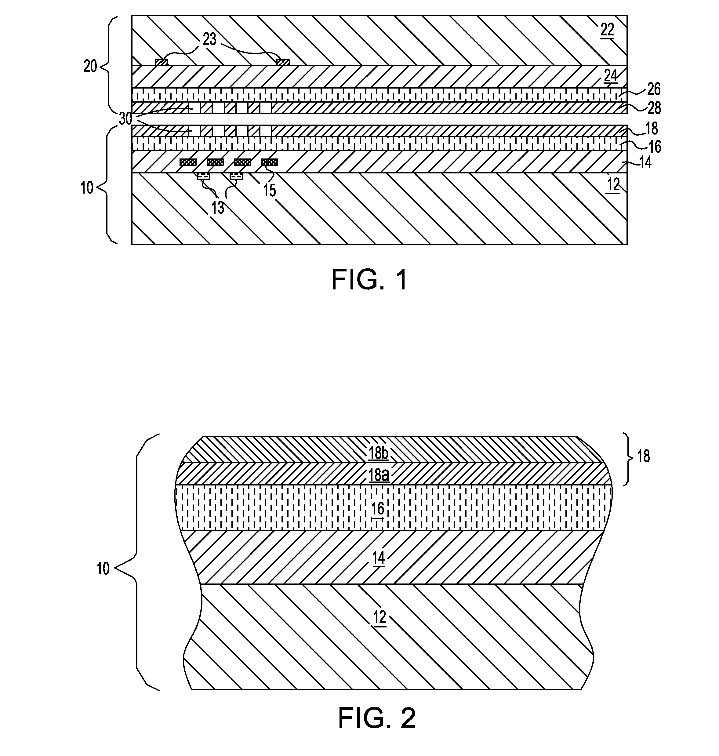
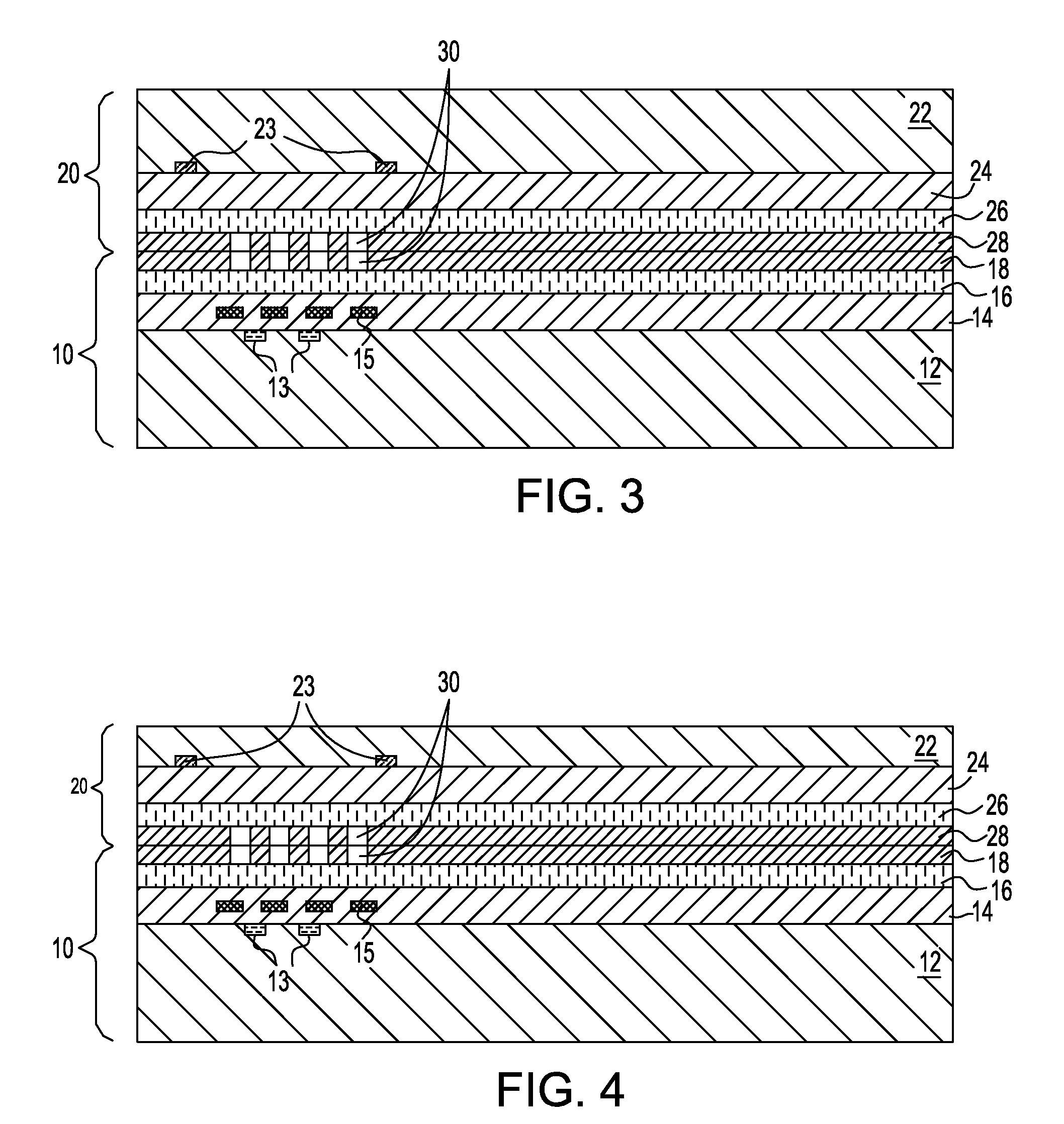
[0042]Referring to the Figures in more detail, and particularly referring to FIG. 1, there is shown a first step in the formation of a 3D integrated circuit structure according to the present invention. First semiconductor structure 10 comprises a semiconductor wafer 12 having integrated circuit devices 13 formed therein. The semiconductor wafer 12 may be made from any semiconductor material including but not limited to group IV semiconductors such as silicon, silicon germanium, or germanium, a III-V compound semiconductor, or a II-VI compound semiconductor.

[0043]The semiconductor wafer 12 has a back end of the line (BEOL) wiring 14 thereon. The BEOL wiring 14 typically includes an insulative material, such as an oxide, and various wiring layers which are well known to those skilled in the art but are not shown for clarity. BEOL wiring 14, however, has a plurality of landing pads 15 which provide connections to the various wiring layers in the BEOL wiring 14.

[0044]Layered on the BEO...


PUM


Abstract

A method of making 3D integrated circuits and a 3D integrated circuit structure. There is a first semiconductor structure joined to a second semiconductor structure. Each semiconductor structure includes a semiconductor wafer, a front end of the line (FEOL) wiring on the semiconductor wafer, a back end of the line (BEOL) wiring on the FEOL wiring, an insulator layer on the BEOL wiring and a metallic layer on the insulator layer. The first semiconductor structure is aligned with the second semiconductor structure such that the metallic layers of each of the semiconductor structures face each other. The metallic layers of each of the semiconductor structures are in contact with and bonded to each other by a metal to metal bond wherein the bonded metallic layers form an electrically isolated layer.

Description

BACKGROUND OF THE INVENTION[0001]The present invention relates generally to three dimensional (3D) integrated circuits, and more particularly to 3D integrated circuits with through silicon vias and the process by which integrated circuits are bonded together.[0002]Since the invention of the integrated circuit, the semiconductor industry has experienced continual rapid growth due to continuous improvements in the integration density of various electronic components (i.e., transistors, diodes, resistors, capacitors, etc.). For the most part, this improvement in integration density has come from repeated reductions in minimum feature size, allowing for the integration of more components into a given area.[0003]These integration improvements are essentially two-dimensional (2D) in nature, in that the volume occupied by the integrated components is essentially on the surface of the semiconductor wafer. Although dramatic improvements in lithography have resulted in considerable improvemen...

Claims


Application Information

Patent Timeline
IPC IPC(8): H01L23/522H01L21/768
CPCH01L21/76898H01L21/8221H01L2224/80896H01L2224/80357H01L2224/80345H01L2924/014H01L24/16H01L24/28H01L24/73H01L24/83H01L24/94H01L25/0657H01L25/50H01L2224/13009H01L2224/13099H01L2224/83201H01L2224/83801H01L2224/83894H01L2225/06513H01L2924/01004H01L2924/01005H01L2924/01013H01L2924/01022H01L2924/01029H01L2924/01032H01L2924/01033H01L2924/01047H01L2924/0105H01L2924/01073H01L2924/01075H01L2924/01078H01L2924/01079H01L2924/01082H01L2924/01322H01L2924/04941H01L2924/04953H01L2924/14H01L2924/19041H01L2924/19043H01L2924/30105H01L2224/80801H01L2924/0132H01L2224/80895H01L2224/9202H01L2924/01006H01L2924/01023H01L24/80H01L24/82H01L24/92H01L2224/82101H01L2224/9212H01L2224/82031H01L2224/05551H01L2224/80986H01L2924/00014H01L2224/80001H01L2224/82
Inventor FAROOQ, MUKTA G.LYER, SUBRAMANIAN S.
Owner TESSERA INC
Why Eureka
Try Eureka