Thin film batteries and methods for manufacturing same

a technology of thin film batteries and manufacturing methods, which is applied in the direction of cell components, final product manufacturing, sustainable manufacturing/processing, etc., can solve the problems of low deposition rate, low throughput, and inability to broad market application of tfbs, and achieves high throughput and yield, facilitates the tfb fabrication process, and improves the effect of tfb manufacturing process

Inactive Publication Date: 2009-11-26
APPLIED MATERIALS INC
View PDF25 Cites 28 Cited by
  • Summary
  • Abstract
  • Description
  • Claims
  • Application Information

AI Technical Summary

Benefits of technology

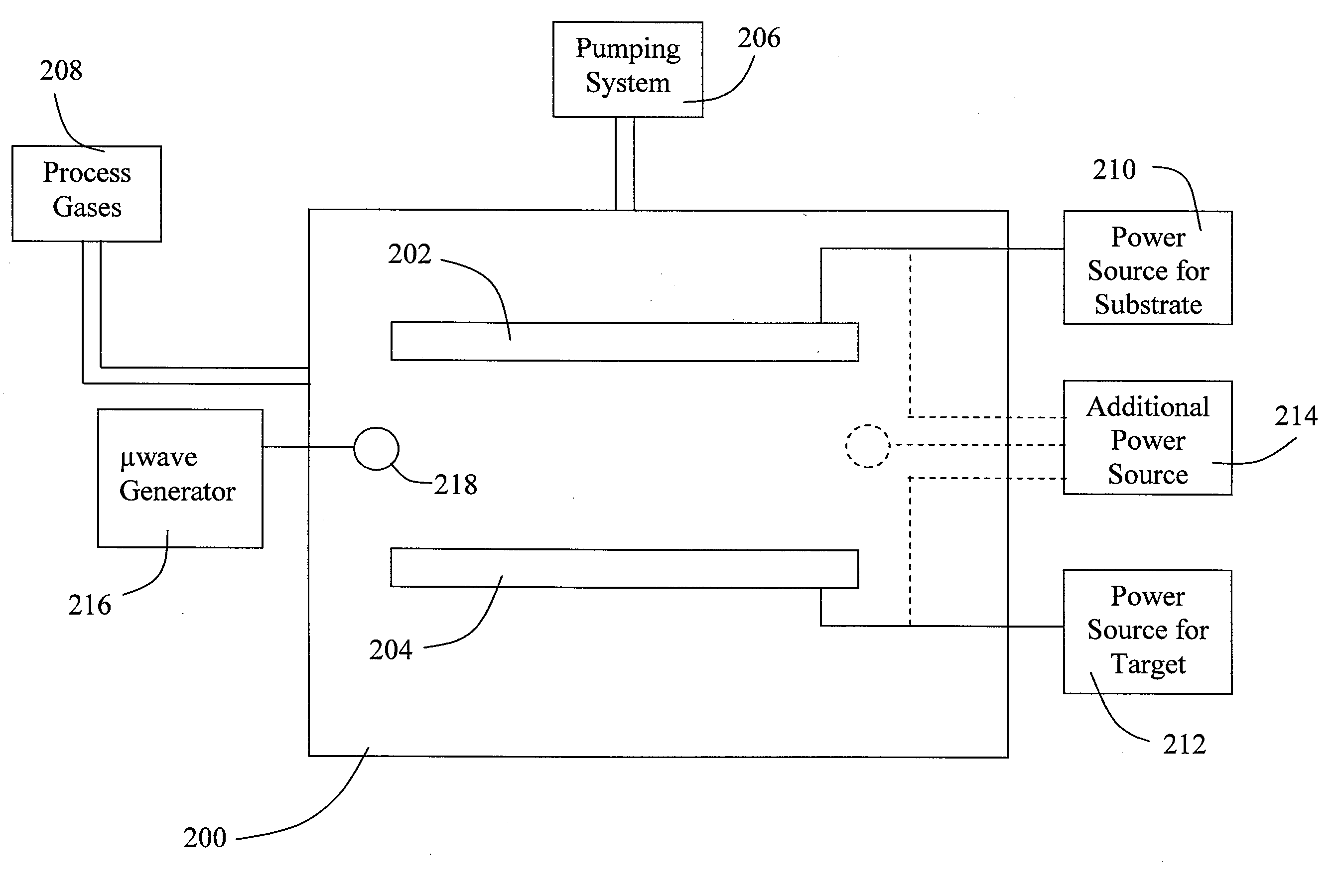
[0015]In another embodiment, the invention provides new deposition sources to facilitate the TFB fabrication process—increasing the throughput and yield. A sputtering target for a thin film battery cathode layer is manufactured to have an average composition of LiMaNbZc, wherein 0.20>{b / (a+b)}>0 and the ratio of a to c is approximately equal to the stoichiometric ratio of a desired crystalline structure of the cathode layer, N is an alkaline earth element, M is selected from the group consisting of Co, Mn, Al, Ni and V, and Z is selected from the group consisting of (PO4), O, F and N. The metals represented by M and the substitutional elements represented by N are not restricted to single species. For example, M may include both Co and Mn. In preferred embodiments, 0.12>{b / (a+b)}>0.05. Furthermore, the target may also comprise other substitutional elements taken from the transition metals in the periodic table. A desirable property of a deposited TFB cathode layer is good crystallinity and relatively high conductivity, whereby post deposition annealing is not required and the layer may be made relatively thick for increased capacity, but without compromising the power (current) density.
[0016]For electrolytes, the addition of energy to the growing film will allow enhanced conformality by allowing additional energy to promote surface diffusion of deposited species. Thus, pinhole free layers can be achieved with lesser thickness. This will help with throughput and battery properties, for example power density or capacity, by reducing the internal impedance.

Problems solved by technology

Most of the past and current state-of-the-art approaches, as they pertain to TFB and TFB fabrication technologies, have been conservative, wherein the efforts have been limited to scaling the basic technologies of the original Oak Ridge National Laboratory inventions that started in the early 1990s.
While some improvements have been made to the original ORNL approaches, there are many problems with the prior art fabrication processes for TFBs that prevent them from being compatible with cost effective and high-volume manufacturing (HVM), and thereby preclude broad market applicability of TFBs.
For example, issues with the state-of-the-art thin film cathode and cathode deposition processes include: (1) a low deposition rate leading to low throughput and inefficient scaling (of economy) for cost reduction, (2) a need for a high temperature anneal for the crystalline phase, which adds to process complexity, low throughput and limitations on the choice of substrate materials, and (3) a higher electrical and ionic resistivity, which limits the thickness of the cathode and high power (in battery operation) application, as well as the applicable sputtering methodology and sputtering power (which determines deposition rate).
With respect to the electrolyte, RF sputtering does not provide a high deposition rate with good conformality for pinhole free deposition.
However, the long term reliability (cycle life) appears less than that observed in TFBs produced with RF sputtered layers.

Method used


Image

  • Thin film batteries and methods for manufacturing same
  • Thin film batteries and methods for manufacturing same
  • Thin film batteries and methods for manufacturing same

Examples


Embodiment Construction

[0020]The present invention will now be described in detail with reference to the drawings, which are provided as illustrative examples of the invention so as to enable those skilled in the art to practice the invention. Notably, the figures and examples below are not meant to limit the scope of the present invention to a single embodiment, but other embodiments are possible by way of interchange of some or all of the described or illustrated elements. Moreover, where certain elements of the present invention can be partially or fully implemented using known components, only those portions of such known components that are necessary for an understanding of the present invention will be described, and detailed descriptions of other portions of such known components will be omitted so as not to obscure the invention. In the present specification, an embodiment showing a singular component should not be considered limiting; rather, the invention is intended to encompass other embodimen...


PUM

PropertyMeasurementUnit
thicknessaaaaaaaaaa
thickaaaaaaaaaa
thickaaaaaaaaaa

Abstract

A method of fabricating a layer of a thin film battery comprises providing a sputtering target and depositing the layer on a substrate using a physical vapor deposition process enhanced by a combination of plasma processes. The deposition process may include: (1) generation of a plasma between the target and the substrate; (2) sputtering the target; (3) supplying microwave energy to the plasma; and (4) applying radio frequency power to the substrate. A sputtering target for a thin film battery cathode layer has an average composition of LiMaNbZc, wherein 0.20>{b/(a+b)}>0 and the ratio of a to c is approximately equal to the stoichiometric ratio of a desired crystalline structure of the cathode layer, N is an alkaline earth element, M is selected from the group consisting of Co, Mn, Al, Ni and V, and Z is selected from the group consisting of (PO4), O, F and N.

Description

FIELD OF THE INVENTION[0001]The present invention relates to thin film batteries, and in particular, improved cathode materials and deposition techniques for certain layers of a thin film battery structure.BACKGROUND OF THE INVENTION[0002]All solid state Thin Film Batteries (TFB) are known to exhibit several advantages over conventional battery technology such as superior form factors, cycle life, power capability and safety. However, there is a need for cost effective and high-volume manufacturing (HVM) compatible fabrication technologies to enable broad market applicability of TFBs.[0003]Most of the past and current state-of-the-art approaches, as they pertain to TFB and TFB fabrication technologies, have been conservative, wherein the efforts have been limited to scaling the basic technologies of the original Oak Ridge National Laboratory inventions that started in the early 1990s. More recently, some efforts to improve the properties and deposition rates for the cathode and elec...

Claims


Application Information

Patent Timeline
Patent Type & Authority Applications(United States)
IPC IPC(8): C23C14/34H01M4/52H01M4/58H01M10/36
CPCC23C14/088C23C14/3414H01M4/0426H01M4/1391Y02E60/122H01M4/5825H01M6/40H01M10/052H01M10/0585H01M4/525Y02E60/10Y02P70/50
Inventor KWAK, BYUNG SUNGSTOWELL, MICHAELKRISHNA, NETY
Owner APPLIED MATERIALS INC
Why Eureka
Try Eureka