Printed circuit board equipped with piezoelectric element

a piezoelectric element and printed circuit board technology, applied in the direction of fixed transformers, circuit electrical arrangements, printed circuit structure associations, etc., can solve the problems of difficult to reduce the size and weight of the wound-rotor electromagnetic transformer, and achieve the effect of low cost and simple structur

Inactive Publication Date: 2010-11-18
CANON KK
View PDF12 Cites 16 Cited by
  • Summary
  • Abstract
  • Description
  • Claims
  • Application Information

AI Technical Summary

Benefits of technology

[0007]The present invention thus aims to solve at least one of such a problem and other problems. For example, the present invention enables a semiconductor component to be protected from discharge with the use of a low-cost and simple method, the discharge being generated from a piezoelectric element due to the pyroelectric effect of the element during a flow soldering process. Note that the other problems will be understood through the entire specification.

Problems solved by technology

The wound-rotor type electromagnetic transformer is, however, difficult to reduce in size and weight.

Method used


Image

  • Printed circuit board equipped with piezoelectric element
  • Printed circuit board equipped with piezoelectric element
  • Printed circuit board equipped with piezoelectric element

Examples


first embodiment

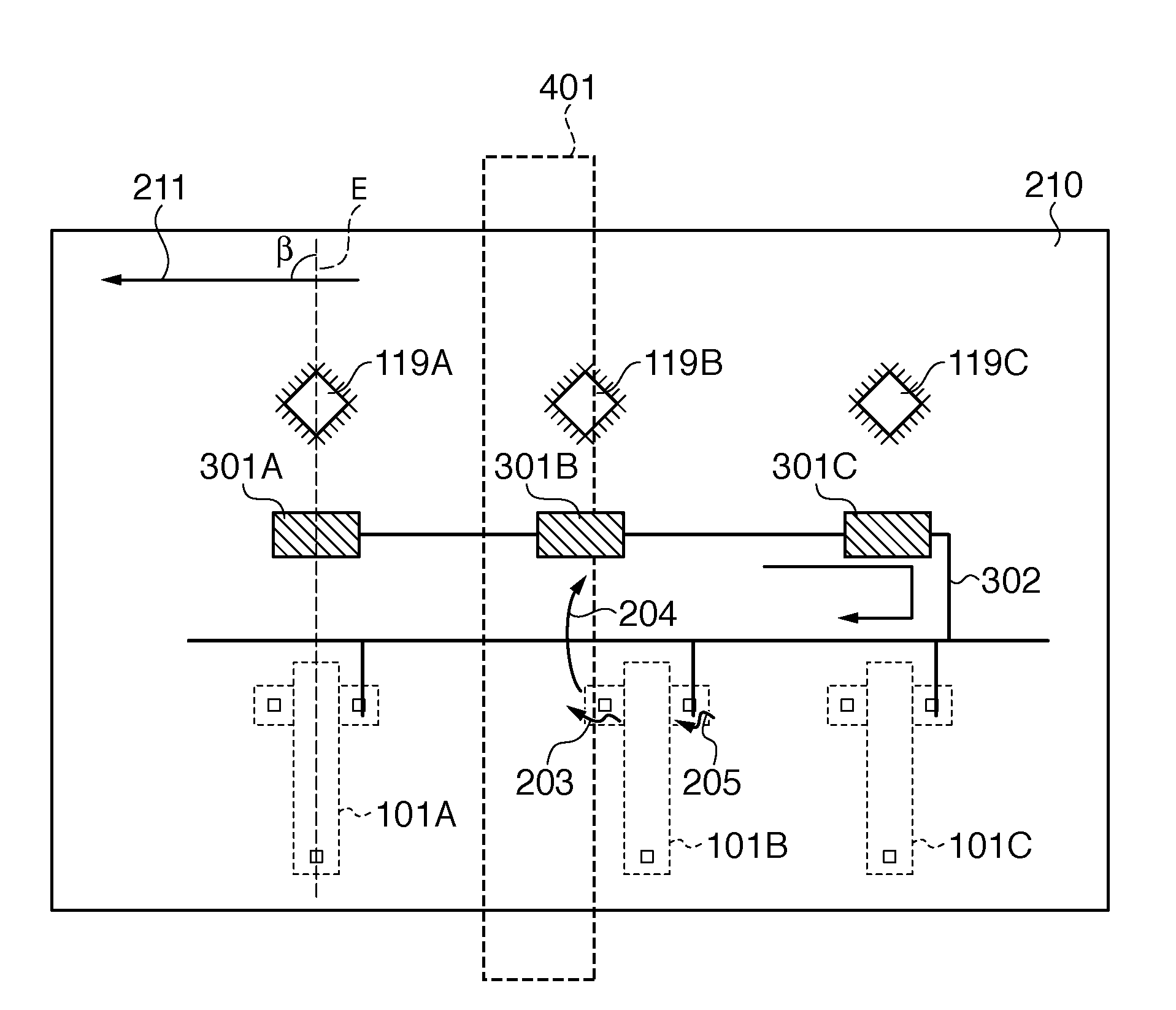
[0047]The present invention is applicable to any electronic apparatus that includes a printed circuit board with a piezoelectric element and a semiconductor component, and the electronic apparatus does not need to be a high-voltage power supply apparatus. The present invention is also effective for a high-voltage power supply apparatus that outputs either a positive or negative voltage. Here, a high-voltage power supply apparatus that outputs a positive voltage will be described by way of example.

[0048]Piezoelectric transformers 101A, 101B, and 101C and semiconductor components 119A, 119B, and 119C illustrated in FIG. 1 are circuit components for forming different circuit blocks. This does not mean that the piezoelectric transformer 101A and the semiconductor component 119A, for example, constitute the same circuit block. In the present embodiment, the piezoelectric transformers 101A, 101B, and 101C and the semiconductor components 119A, 119B, and 119C are located parallel to a trav...

second embodiment

[0055]In the first embodiment, the semiconductor components are protected from discharge by providing the solder lands 301A, 301B, and 301C between the semiconductor components and the piezoelectric elements. In a second embodiment, a soldering enabling pattern is adopted instead of the solder lands 301A, 301B, and 301C.

[0056]A soldering enabling pattern 303 illustrated in FIG. 3 is a kind of land formed by exposing a wiring portion of a reference potential pattern 302. A single or multiple soldering enabling patterns 303 are located generally in parallel with a board travelling direction (the direction indicated by arrow 211) during solder mounting. That is, the soldering enabling pattern 303 that is part of a reference potential pattern and that extends in the travelling direction of a printed circuit board during the soldering process is adopted as a land that forms part of a discharge path. To simplify the description, FIG. 3 illustrates a single soldering enabling pattern 303. ...

third embodiment

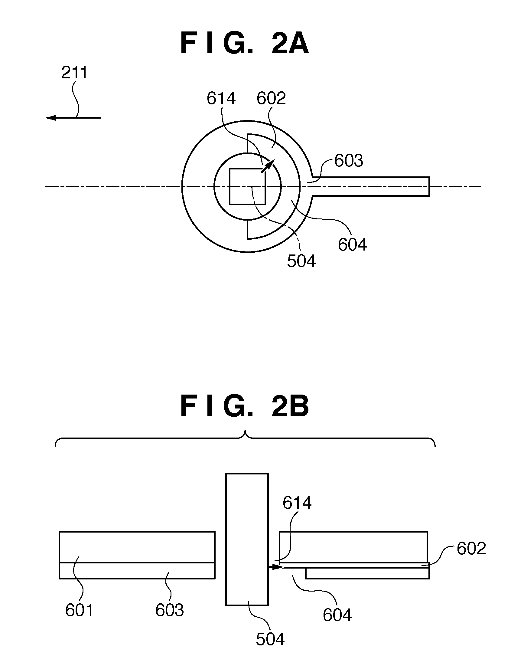
[0058]A major difference of a third embodiment illustrated in FIG. 4 from the first and second embodiments is that anti-solder bridging patterns 304A, 304B, and 304C that are provided at end portions of semiconductor components are adopted as a discharge path in order to restrain the occurrence of solder bridging during the soldering process. Note that the anti-solder bridging patterns 304A, 304B, and 304C may also be referred to as dummy lands or dummy pads. The anti-solder bridging patterns 304A, 304B, and 304C are connected to ground lines or power supply lines through which a reference potential is given to semiconductor components. Note that the anti-solder bridging patterns 304A, 304B, and 304C are formed by stripping off a resist 603 and thereby exposing a copper foil 602 of wiring portions.

[0059]As described above, the anti-solder bridging patterns 304A, 304B, and 304C connected to a reference potential pattern are provided between the semiconductor components and the piezoe...


PUM


Abstract

An electronic apparatus includes, for example, a circuit board with an electronic component and a piezoelectric element, a reference potential pattern that gives a reference potential to at least one of the electronic component and the piezoelectric element, and a solder land connected to the reference potential pattern. On the circuit board, the electronic component is located on a downstream side in a transport direction of the circuit board during mounting of the piezoelectric element and the electronic component on the solder land, and the piezoelectric element is located on an upstream side in the transport direction.

Description

BACKGROUND OF THE INVENTION[0001]1. Field of the Invention[0002]The present invention relates to a printed circuit board with piezoelectric elements.[0003]2. Description of the Related Art[0004]In an electrophotographic image forming apparatus, for good image transfer to a sheet, a high voltage (a voltage of several hundred volts or more, which is higher than a commercial power supply voltage) is generally applied to a transfer roller, and a current of approximately 10 μA is applied to the transfer roller. To generate such a high voltage, conventionally a wound-rotor type electromagnetic transformer has been used. The wound-rotor type electromagnetic transformer is, however, difficult to reduce in size and weight. To further reduce the size and weight of an electronic apparatus such as an image forming apparatus, the size and weight of a power supply that generates a high voltage must be reduced. To achieve a reduction in the size and weight of a power supply, the use of a piezoelec...

Claims


Application Information

Patent Timeline
Patent Type & Authority Applications(United States)
IPC IPC(8): H05K7/02
CPCG03G15/80H05K1/0259H01L2924/0002H05K1/111H05K1/116H05K3/3447H05K3/3452H05K3/3468H05K2201/09463H05K2201/09781H05K2201/09854H05K2201/099H05K2201/10083H05K2201/10689H05K2201/1081H05K2203/046H05K2203/044H01L2924/00
Inventor NAGASAKI, OSAMU
Owner CANON KK
Why Eureka
Try Eureka