Method for providing electrical connections to spaced conductive lines

a technology of electrical connections and conductive lines, applied in the direction of electrical apparatus, semiconductor devices, semiconductor/solid-state device details, etc., can solve the problems of inability to reliably form line features, limit the ability to make electrical connections to a particular line without such known photolithographic techniques, and the inability to accurately patterned lines

Active Publication Date: 2010-11-25
MICRON TECH INC
View PDF10 Cites 12 Cited by
  • Summary
  • Abstract
  • Description
  • Claims
  • Application Information

AI Technical Summary

Problems solved by technology

There are limitations on how close line features, such as conductive lines, can be patterned using such known photolithographic techniques.
Due to factors such as optics and light or radiation wavelength, there is a minimum pitch below which line features cannot be reliably formed using conventional photolithographic techniques.
As techniques such as double patterning, spacer pitch doubling, and BCP self-assembly enable the creation of more closely spaced conductive lines, it becomes increasingly difficult to make an electrical connection to a particular line without overlapping and shorting between adjacent lines.
Present lithography technology does not have the resolution or alignment capability to print the patterns necessary to make connection sites for these smaller features.

Method used


Image

  • Method for providing electrical connections to spaced conductive lines
  • Method for providing electrical connections to spaced conductive lines
  • Method for providing electrical connections to spaced conductive lines

Examples


Embodiment Construction

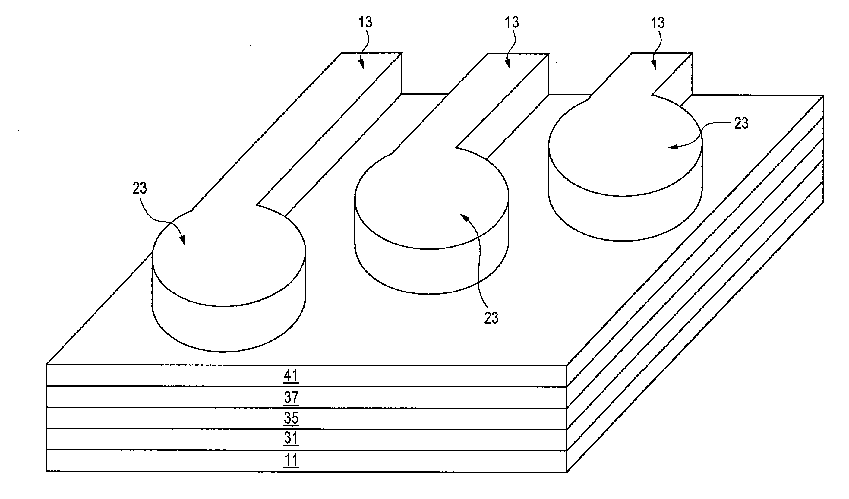
[0030]Embodiments described herein address the problems with current techniques for making electrical connections to closely spaced conductive lines, e.g. parallel lines with spacing of less than 45 nm in width, and provide electrical connections to such closely spaced conductive lines. The embodiments described herein can also be used to make electrical connections to any spaced conductive lines including those formed using conventional photolithographic techniques.

[0031]It should be understood that embodiments of the invention are not limited by the example embodiments described herein and that changes can be made thereto. The embodiments described herein can be applied to any integrated circuit that has spaced lines, and is particularly suitable for making connections to parallel conductive lines including closely spaced parallel conductive lines, for example, parallel conductive lines having a spacing of 45 nm or less between them, and more particularly to such conductive lines ...


PUM


Abstract

An integrated circuit and a method of formation provide a contact area formed at an angled end of at least one linearly extending conductive line. In an embodiment, conductive lines with contact landing pads are formed by patterning lines in a mask material, cutting at least one of the material lines to form an angle relative to the extending direction of the material lines, forming extensions from the angled end faces of the mask material, and patterning an underlying conductor by etching using said material lines and extension as a mask. In another embodiment, at least one conductive line is cut at an angle relative to the extending direction of the conductive line to produce an angled end face, and an electrical contact landing pad is formed in contact with the angled end face.

Description

FIELD OF THE INVENTION[0001]Embodiments described herein relate generally to the fabrication of integrated circuits, and more specifically to providing electrical connections to spaced conductive lines, e.g. spaced parallel lines, in integrated circuits.BACKGROUND OF THE INVENTION[0002]Electrically conductive lines form many common components of integrated circuits. Dynamic random access memory (DRAM) circuitry, for example, incorporates multiple parallel conductive lines to form wordlines and bitlines. In order to increase capacity and accommodate smaller devices, there is constant pressure to increase the density of components on these and other circuits. The continual reduction in feature sizes places greater demands on the techniques used to form the features.[0003]Photolithography is a commonly used technique for patterning integrated circuit features. One example of a photolithographic method for forming conductive lines using conventional photolithographic techniques is illus...

Claims


Application Information

Patent Timeline
Patent Type & Authority Applications(United States)
IPC IPC(8): H01L23/48H01L21/50
CPCH01L21/32139H01L21/76895H01L23/528H01L27/10885H01L27/10891H01L2924/12044H01L21/76877H01L21/823871H01L2224/06138H01L23/5283H01L21/28008H01L21/28518H01L21/3081H01L21/76885H10B12/488H10B12/482H01L21/768H10B99/00H10B12/00H10B12/485H01L21/28035
Inventor SANDHU, GURTEJSILLS, SCOTT
Owner MICRON TECH INC
Why Eureka
Try Eureka