Interference reduction device

a technology of interference reduction and reduction device, which is applied in the field of interference reduction device, can solve the problems of large noise and communication quality deterioration, difficult to take this measure in the layout process, and lower exerted error correction performance than the intrinsic performance level of error correction cod

Inactive Publication Date: 2010-11-25
KK TOSHIBA
View PDF4 Cites 60 Cited by
  • Summary
  • Abstract
  • Description
  • Claims
  • Application Information

AI Technical Summary

Benefits of technology

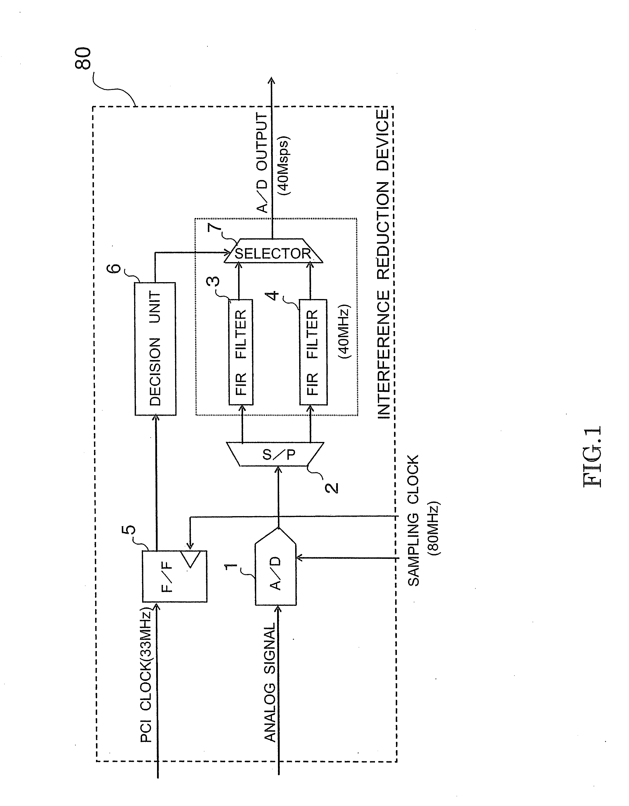
[0005]According to an aspect of the invention is provided an interference reduction device, comprising an analog to digital converter (A / D converter: ADC) to perform A / D conversion on input analog signal at frequency twice as high as output frequency, a serial to parallel converter (S / P converter) to repeatedly perform a session of distribution processing in which a digital signal obtained by the A / D conversion is distributed on a symbol basis to two destinations in a predetermined order, a digital filter to receive the signal distributed at the first timing in each session of the distribution processing and to output the signal after a filer operation at the output frequency, an interpolation filter to receive the signal other than the signal distributed at the first timing in each session of the distribution processing, to perform a filter operation, also to perform interpolation processing to thereby generate the signal distributed to the digital filter in the distribution processing, and to output the generated signal at the output frequency, a sampling unit to sample the inputted digital signal at frequency twice as high as the output frequency, a decision unit to decide which one of the digital filter and the interpolation filter has received smaller influence of interference of the input digital signal, on the basis of a sampling result by the sampling unit, and a selector to output one of the signals outputted by the digital filter and the interpolation filter, on the basis of a decision result of the decision unit.
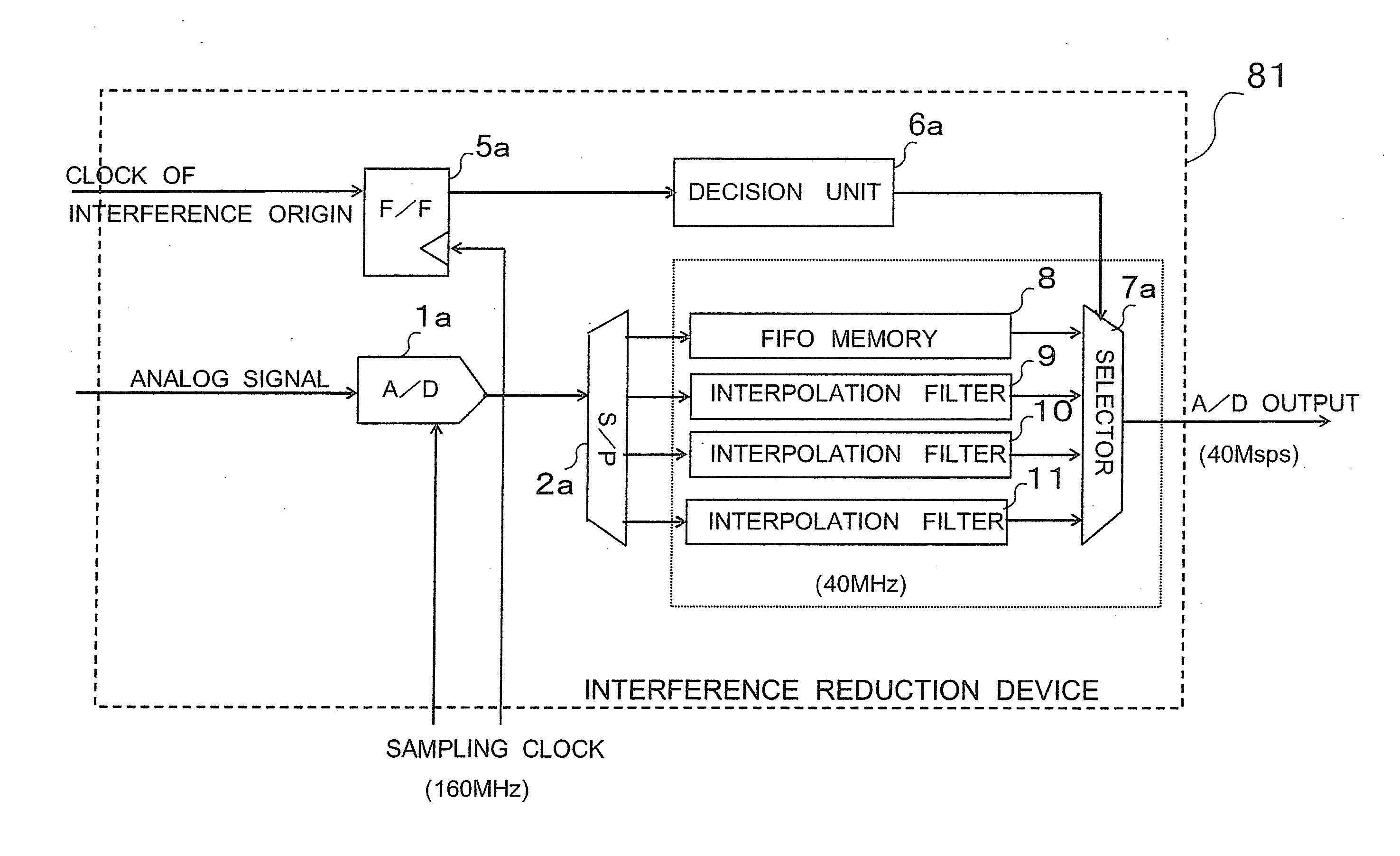
[0006]According to another aspect of the invention is provided an interference reduction device, comprising an analog to digital converter (A / D converter: ADC) to perform A / D conversion on input analog signal at frequency M (M is an integer of 3 or more) times as high as output frequency, a serial to parallel converter (S / P converter) to repeatedly perform a session of distribution processing in which a digital signal obtained by the A / D conversion is distributed on a symbol basis to M destinations in a predetermined order, a digital filter to receive the signal distributed at the first timing in each session of the distribution processing and to output the signal after a filer operation at the output frequency, (M-1) interpolation filters each to receive the signal other than the signal distributed at the first timing in each session of the distribution processing, to perform a filter operation, also to perform interpolation processing to thereby generate the signal distributed to the digital filter in the distribution processing, and to output the generated signal at the output frequency, a sampling unit to sample the inputted digital signal at frequency M times as high as the output frequency, a decision unit to decide which one of the digital filter and the (M-1) interpolation filters has the smallest influence of interference of the input digital signal, on the basis of a sampling result by the sampling unit, and a selector to output one of the signals outputted by the digital filter and the (M-1) interpolation filters, on the basis of a decision result of the decision unit.
[0007]According to another aspect of the invention is provided an interference reduction device, comprising an analog to digital converter (A / D converter: ADC) to perform A / D conversion on input analog signal at frequency M (M is an integer of 3 or more) times as high as output frequency, a serial to parallel converter (S / P converter) to repeatedly perform a session of distribution processing in which a digital signal obtained by the A / D conversion is distributed on a symbol basis to M destinations in a predetermined order, a buffer to receive the signal distributed at the first timing in each session of the distribution processing and to output the symbols in a first-in first-out order, (M-1) interpolation filters each to receive the signal other than the signal distributed at the first timing in each session of the distribution processing, to perform a filter operation, also to perform interpolation processing to thereby generate the signal distributed to the buffer in the distribution processing, and to output the generated signal at the output frequency, a sampling unit to sample the inputted digital signal at frequency M times as high as the output frequency, a decision unit to decide which one of the buffer and the (M-1) interpolation filters has received the smallest influence of interference of the input digital signal, on the basis of a sampling result by the sampling unit; and a selector to output one of the signals outputted by the buffer and the (M-1) interpolation filters, on the basis of a decision result of the decision unit.

Problems solved by technology

Heretofore, a communication apparatus has the following problem in digital modulation if an analog signal line and an asynchronous digital signal line are arranged close to each other in the communication apparatus.
Consequently, the resultant data includes large noise and communication quality deteriorates.
However, an increase in the integration degree makes it difficult to take this measure in the layout process.
However, when the error correction code is used to correct a signal influenced by the interference, the exerted error correction performance is lower than the intrinsic performance level of the error correction code.
However, these techniques have a drawback in that the techniques can produce the effects by only when a digital signal of interference origin and sampling clock are synchronous with each other, but cannot obtain good communication quality when the digital signal and the sampling clock are asynchronous with each other.

Method used


Image

  • Interference reduction device
  • Interference reduction device
  • Interference reduction device

Examples


Embodiment Construction

[0023]Hereinafter, interference reduction devices according to embodiments of the invention will be described with reference to the accompanying drawings.

[0024]An interference reduction device according to a first embodiment of the invention will be described with reference to the accompanying drawings. FIG. 1 is a diagram showing a configuration example of the interference reduction device. As shown in FIG. 1, an interference reduction device 80 includes an analog-to-digital converter (A / D converter: “ADC”) 1, a serial-to-parallel converter (S / P converter) 2, a finite impulse response (FIR) filter 3, a FIR filter 4, a flip-flop 5, a decision unit 6, and a selector 7.

[0025]The A / D converter 1 converts an analog signal into a digital signal. Here, a sampling clock is set at 80 MHz. The S / P converter 2 performs serial-to-parallel conversion on symbols outputted from the A / D converter 1. The FIR filter 3 and the FIR filter 4 are digital filters in use. The FIR filter 4 performs interpo...


PUM


Abstract

An interference reduction device includes an analog to digital converter, a serial to parallel converter, a first FIR filter, a second FIR filters, a flip-flop, a decision unit, and a selector. The analog to digital converter performs A/D conversion. The serial to parallel converter performs a session of distribution processing in which a digital signal obtained by the A/D conversion. The first FIR outputs the signal after a filer operation at the desired output frequency. The second FIR filters each perform a filter operation, also each output the generated signals at the desired output frequency. The flip-flop samples the inputted digital signal. The decision unit decides which one of the FIR filters has the smallest influence of interference of the input digital signal. The selector outputs one of the signals outputted by the FIR filters.

Description

CROSS REFERENCE TO RELATED APPLICATION[0001]This application is based upon and claims the benefit of priority from the prior Japanese Patent Application No.P2009-121162, filed on May 19, 2009, the entire contents of which are incorporated herein by reference.FIELD OF THE INVENTION[0002]The present invention relates to an interference reduction device to reduce interference with an analog signal from a digital signal.DESCRIPTION OF THE BACKGROUND[0003]Heretofore, a communication apparatus has the following problem in digital modulation if an analog signal line and an asynchronous digital signal line are arranged close to each other in the communication apparatus. More specifically, such close arrangement allows toggles in the digital signal to interfere with the analog signal, and thereby sharp peaks sometimes appear in the analog signal. When the analog signal thus influenced by the interference is sampled, the peaks are also taken into the samples. Consequently, the resultant data ...

Claims


Application Information

Patent Timeline
Patent Type & Authority Applications(United States)
IPC IPC(8): H03M1/12
CPCH03M1/0656H03M1/12H03M1/0863H03M1/0827
Inventor YAMAKI, RYOYAMAGISHI, TOSHIYUKI
Owner KK TOSHIBA
Why Eureka
Try Eureka