Organic electroluminescence display device and manufacturing method thereof

a technology of electroluminescence display and manufacturing method, which is applied in the direction of static indicating devices, solid-state devices, instruments, etc., can solve the problems of increasing the number of manufacturing schemes, increasing the cost of the buffer-layer forming system, and increasing the cost of the depositing system, so as to reduce the wiring resistance, reduce the number of luminance variations, and high display quality

Active Publication Date: 2010-12-02
JOLED INC
View PDF34 Cites 64 Cited by
  • Summary
  • Abstract
  • Description
  • Claims
  • Application Information

AI Technical Summary

Benefits of technology

[0026]The present invention can realize an organic EL display device having high displaying quality, the organic EL display device which prevents an overcurrent from flowing into a pixel, and has significantly few luminance variations, even on a large pane

Problems solved by technology

The process also results in an increasing cost of the depositing system in order to satisfy the specifications including a process to stabilize the evaporating speeds.
As described above, realizing the luminescent

Method used


Image

  • Organic electroluminescence display device and manufacturing method thereof
  • Organic electroluminescence display device and manufacturing method thereof
  • Organic electroluminescence display device and manufacturing method thereof

Examples


embodiment 1

[0091]Described shall be an organic electroluminescence display device (hereinafter referred to as an organic EL display device) in accordance with Embodiment 1 of the present invention with reference to the drawings.

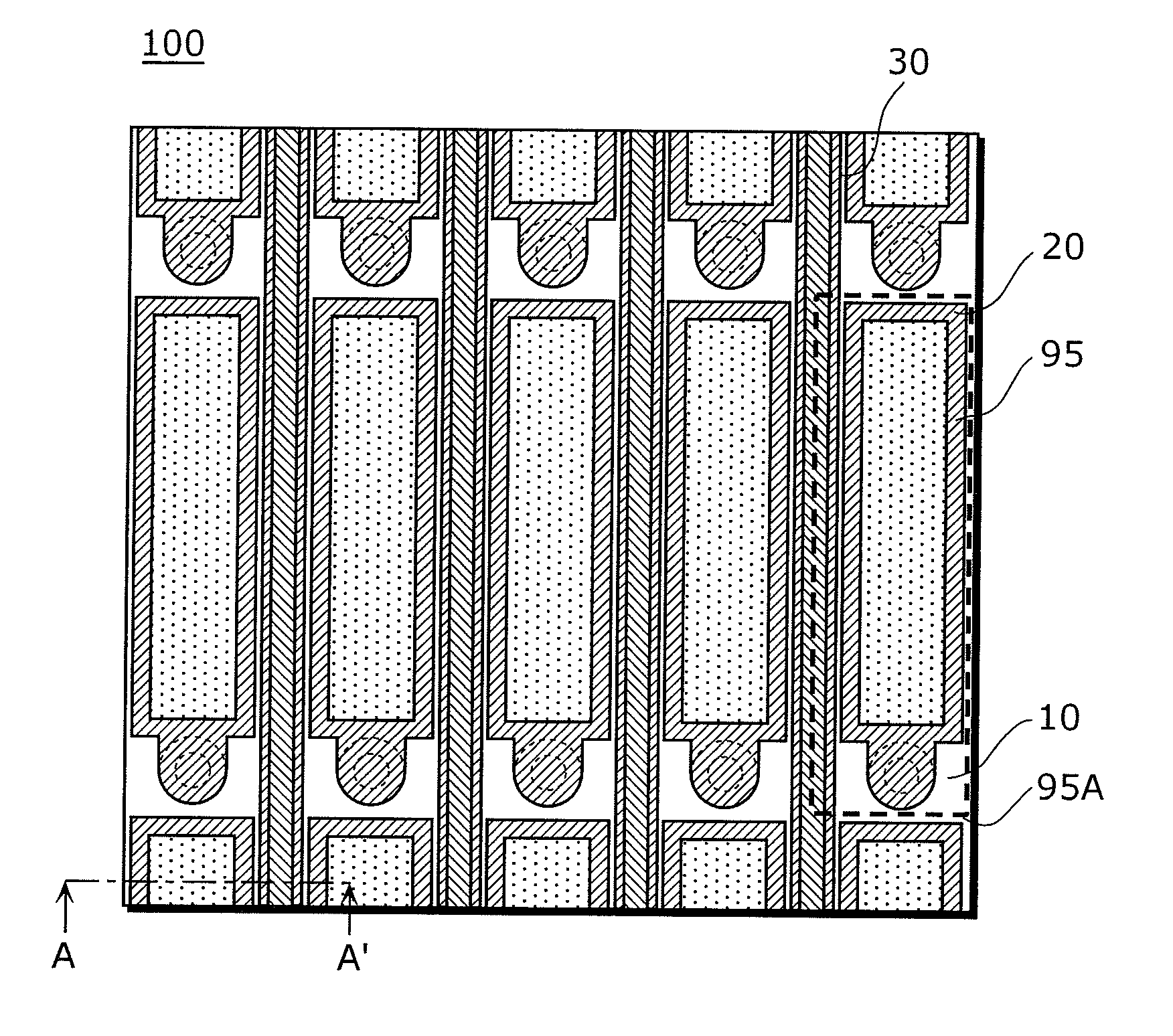
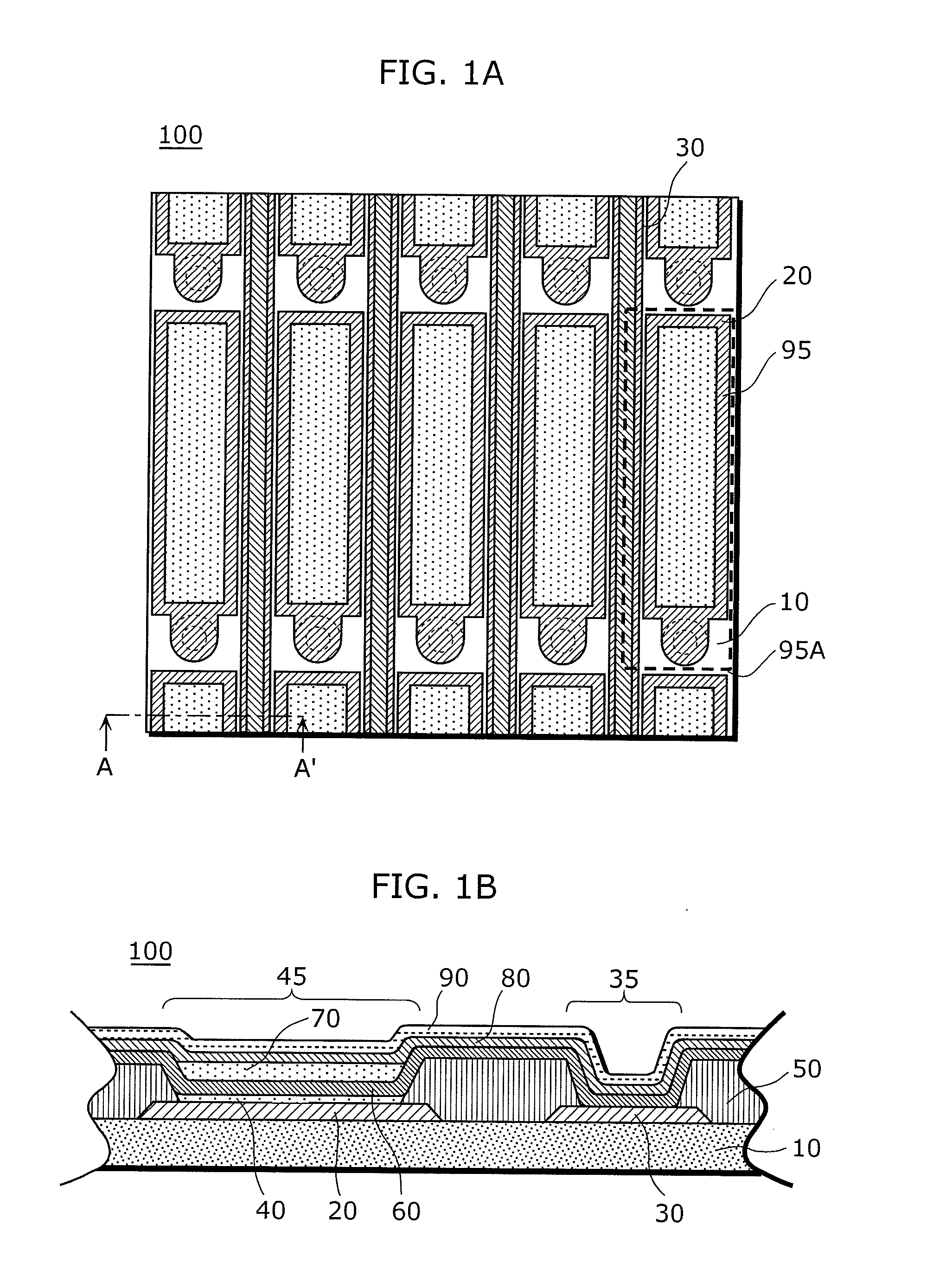
[0092]FIG. 1A is a partial plan view illustrating a main section of the organic EL display device in accordance with Embodiment 1 of the present invention. FIG. 1B is a cross-sectional view, of the main section, taken from line IA-IA of FIG. 1A.

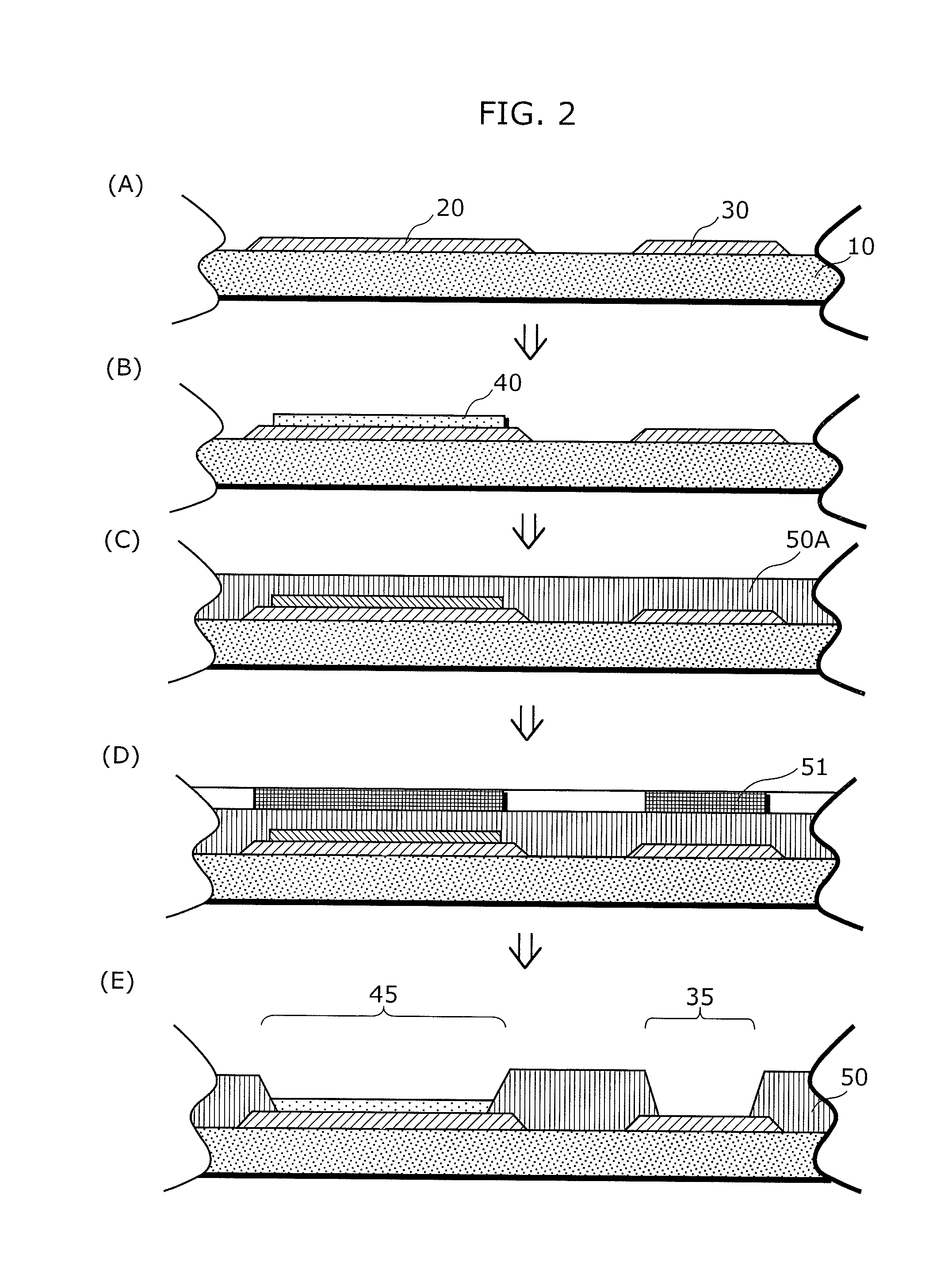
[0093]An organic EL display device 100, in accordance with Embodiment 1, illustrated in substrate FIG. 1B includes: a substrate 10; a first electrode 20 and an auxiliary wire 30 provided on the substrate 10; a hole injection layer 40 provided on the first electrode 20; a barrier 50 forming a pixel opening part 45 and a connection opening part 35; a hole transport layer 60 provided over the substrate 10, the first electrode 20, the auxiliary wire 30, the hole injection layer 40, and the barrier 50; a luminescent layer 70 provided ...

embodiment 2

[0150]Described hereinafter shall be an organic EL display device in accordance with Embodiment 2 of the present invention with reference to the drawings.

[0151]FIG. 7 is a partial plan view illustrating a main section of an organic EL display device in accordance with Embodiment 2 of the present invention. As shown in FIG. 7, an organic EL display device 300 includes a substrate 11 and a displaying unit 100A. The substrate 11 includes a driving circuit layer 111 forming a driving element driving a luminescent unit, and an interlayer insulating layer 112 formed on the driving circuit layer 111. In addition, the displaying unit 100A corresponds to the structural elements of the organic EL display device 100 illustrated in FIG. 1B other than the substrate 10. The organic EL display device 300 in accordance with Embodiment 2 is different from the organic EL display device 100 in accordance with Embodiment 1 in substrate structure. Described hereinafter are only the differences between t...

embodiment 3

[0160]Described hereinafter shall be an organic EL display device in accordance with Embodiment 3 of the present invention with reference to the drawings.

[0161]FIG. 9A is a partial plan view illustrating a main section of the organic

[0162]EL display device in accordance with Embodiment 3 of the present invention. FIG. 9B is a cross-sectional view, of the main section, taken from line IXA-IXA of FIG. 9A.

[0163]As shown in FIG. 9B, the organic EL display device 400 in accordance with Embodiment 3 includes: a substrate 12; the first electrode 20 provided on the substrate 12; an auxiliary wire 33 provided in the substrate 12; the hole injection layer 40 provided on the first electrode 20; the barrier 50 forming the pixel opening part 45 and the connecting opening part 35; the hole transport layer 60 provided over the substrate 12, the first electrode 20, the auxiliary wire 33, the hole injection layer 40, and the barrier 50; the luminescent layer 70 provided in the pixel opening part 45;...


PUM

PropertyMeasurementUnit
Thicknessaaaaaaaaaa
Thicknessaaaaaaaaaa
Nanoscale particle sizeaaaaaaaaaa

Abstract

An organic electroluminescence display includes a first electrode and an auxiliary wire each either on or in a substrate. A luminescent layer is over the first electrode, and a hole transport layer is between the luminescent layer and the first electrode. The hole transport layer extends from over the first electrode to over the auxiliary wire. A second electrode is over the luminescent layer and extends from over the first electrode to over the auxiliary wire. A metal layer is over the auxiliary wire between the hole transport layer and the second electrode. The second electrode and the auxiliary wire are electrically connected via the hole transport layer and the metal layer. The metal layer comprises a metal, wherein a difference of a work function value of the metal minus an absolute value of an energy level of a lowest unoccupied molecular orbit of the hole transport layer is at most approximately 0.5 eV.

Description

CROSS REFERENCE TO RELATED APPLICATION[0001]This is a continuation application of PCT Application No. PCT / JP2009 / 005490 filed Oct. 20, 2009, designating the United States of America, the disclosure of which, including the specification, drawings, and claims, is incorporated herein by reference in its entirety.[0002]The disclosure of Japanese Patent Application No. 2008-322882 filed on Dec. 18, 2008 including specification, drawings and claims is incorporated herein by reference in its entirety.BACKGROUND OF THE INVENTION[0003]1. Field of the Invention[0004]The present invention relates to display devices employing organic electroluminescence (EL) elements and manufacturing methods thereof, in particular, to a display device with luminance variation of an organic EL element reduced, and a manufacturing method thereof.[0005]2. Description of the Related Art[0006]Recent years have seen a rapidly increasing demand for flat-screen display devices such as a flat-screen liquid crystal disp...

Claims


Application Information

Patent Timeline
IPC IPC(8): G09G3/30G09G5/00H01L51/52
CPCH01L27/3246H01L51/0037H01L51/0068H01L51/0069H01L51/0079H01L51/0085H10K59/122H10K85/1135H10K85/656H10K85/655H10K85/321H10K85/342H10K50/15
Inventor OKUMOTO, KENJI
Owner JOLED INC
Why Eureka
Try Eureka