
Method of applying the analysis of scrub mark morphology and location to the evaluation and correction of semiconductor testing, analysis, and manufacture

Inactive Publication Date: 2010-12-02
ONTO INNOVATION INC
View PDF16 Cites 4 Cited by
  • Summary
  • Abstract
  • Description
  • Claims
  • Application Information

AI Technical Summary

Benefits of technology

[0009]By examining scrub mark properties (such as position and size) directly, the performance of a wafer probing process may be evaluated. Scrub mark images are captured, image d

Problems solved by technology

It is well known that scrub patterns analyzed by a probe card analysis machine do not match the scrub marks produced on a test wafer imaged by a scrub mark analysis machine.
Furthermore, the place at which the probe pin first contacts an aluminized bonding pad (or the aluminized semiconductor test wafer which simulates the bonding pad in the scrub mark analysis machine) or “touch downs position of the probe pin is not readily discernable in the scrub mark made in the aluminum surface.

Method used


Image

  • Method of applying the analysis of scrub mark morphology and location to the evaluation and correction of semiconductor testing, analysis, and manufacture
  • Method of applying the analysis of scrub mark morphology and location to the evaluation and correction of semiconductor testing, analysis, and manufacture
  • Method of applying the analysis of scrub mark morphology and location to the evaluation and correction of semiconductor testing, analysis, and manufacture

Examples


Embodiment Construction

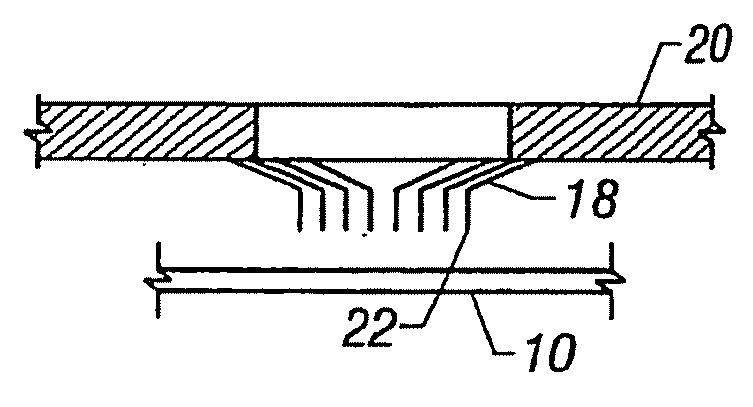
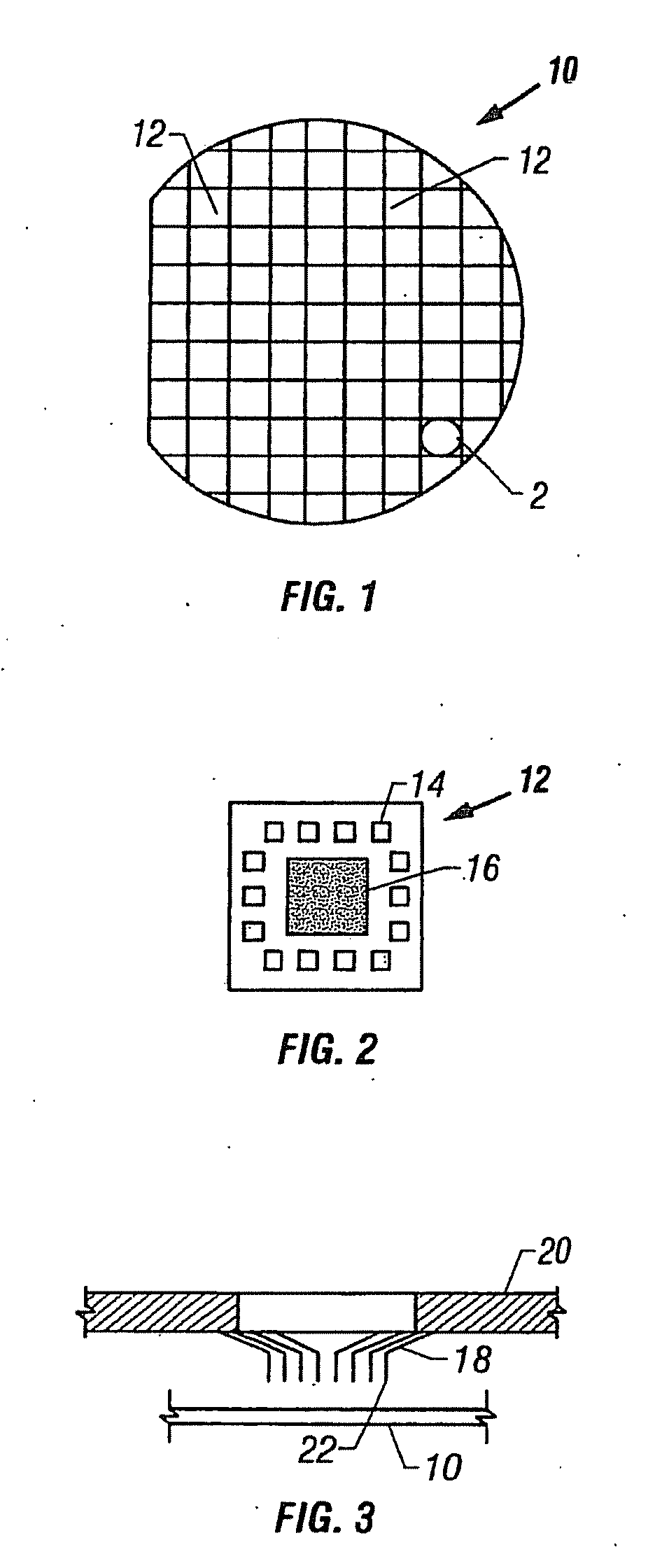
[0022]A semiconductor wafer is generally indicated at reference numeral 10 in FIG. 1. A semiconductor wafer has a plurality of dies 12 arranged in orthogonal rows and columns across the surface of the wafer. A conventional wafer may have a diameter of up to eight inches and anywhere from 200 up to thousands of dies per wafer depending upon the complexity of the semiconductor circuits imbedded in each die. A representative die is generally indicated at reference number 12 in FIG. 2. The die has a plurality of bonding pads 14 and a plurality of semiconductor circuits 16 surrounded by the bonding pads. The bonding pads typically have an aluminized, copper, gold bump, solder bump, or similarly annealed surface. The bonding pads serve as an electrical intermediary between the world outside of the integrated circuit 16 and the circuit itself. Small wires (not shown) interconnect the bonding pads 14 with the semiconductor circuit 16. Another set of small wires (also not shown) interconnect...


PUM


Abstract

By examining scrub mark properties (such as position and size) directly, the performance of a wafer probing process may be evaluated. Scrub mark images are captured, image data measured, and detailed information about the process is extracted through analysis. The information may then be used to troubleshoot, improve, and monitor the probing process.

Description

CROSS-REFERENCE TO RELATED APPLICATIONS[0001]The present application is a continuation of and claims benefit of priority from U.S. application Ser. No. 11 / 479,822, filed Jun. 29, 2006, which is a continuation of U.S. Pat. No. 7,102,368, issued Sep. 5, 2006, which is a continuation of now abandoned U.S. application Ser. No. 10 / 046,559, filed Oct. 27, 2001, which claimed benefit of now abandoned U.S. Provisional Application Ser. No. 60 / 244,432, filed Oct. 30, 2000, the contents of which are each incorporated herein by reference.TECHNICAL FIELD[0002]Aspects of the present invention relate generally to semiconductor testing equipment, and more specifically, to methods of analyzing scrub marks.BACKGROUND OF THE INVENTION[0003]A variety of equipment and techniques have been developed to assist manufacturers of integrated circuits for testing those circuits while still in the form of dies on semiconductor wafers. In order to quickly and selectively electrically interconnect metalized conta...

Claims


Application Information

Patent Timeline
IPC IPC(8): G01R35/00G01R31/26G06F19/00G01R1/067G01R1/073G01R31/28
CPCG01R1/06794G01R1/07342G01R35/00G01R31/2891G01R31/2886
Inventor STROM, JOHN T.
Owner ONTO INNOVATION INC
Features
  • Generate Ideas
  • Intellectual Property
  • Life Sciences
  • Materials
  • Tech Scout
  • Unparalleled Data Quality
  • Higher Quality Content
  • 60% Fewer Hallucinations
Learn More