Ultrasonic probe

a technology of ultrasonic probes and probes, which is applied in the field of ultrasonic probes, can solve the problems of increasing the crystal impedance (ci) and degrading the resonating characteristic, and achieve the effect of small probability of crystal element chipping

Inactive Publication Date: 2010-12-16
NIHON DEMPA KOGYO CO LTD
View PDF7 Cites 1 Cited by
  • Summary
  • Abstract
  • Description
  • Claims
  • Application Information

AI Technical Summary

Benefits of technology

[0019]According to this type of configuration, on both sides of the +X-axis one end section of the crystal element, there is provided the mask that corresponds to the projecting sections extending in the −X-axis direction. Consequently, as with the conventional example, etching from both sides of the one end section of the crystal element (rectangular) is prevented. Moreover the crystal element is etched from the tip end of the projecting section extending in the +X-axis. Therefore, after the outer-shape processing of the crystal element by means of etching has been completed (at the time of completion), the triangular inclined surfaces due to the anisotropy of etching in both of the corner sections of the crystal element can be made small. Furthermore the projecting sections on both sides of the one end sections are distanced from the frame section after etching. Therefore, they do not need to be mechanically separated from the frame section after the etching. Consequently, mechanical separation only occurs at the supporting section, and therefore the probability of chipping occurring in the crystal element becomes small.
[0020]In the present invention, the projecting sections of the first mask join with the frame section, and are made smaller than the width of the supporting section. Thereby, when etching the crystal wafer, in a state where the supporting section is joined with the frame section, the etching is conducted while forming the triangular inclined surfaces with projecting sections separated from the frame section and the tip ends of the respective corner sections as the apex. Therefore, after the etching of the crystal element has been conducted, the inclined surfaces on both sides of the one end section of the crystal element (rectangular) become small.
[0021]Moreover, in the present invention, the projecting sections of the first mask are preliminarily made distanced from the frame section. Also in this case, etching is conducted while forming triangular inclined surfaces with the apexes on the tip ends of the respective corner sections on both sides of the one end section where the projecting sections are provided. Therefore, after the outer-shape processing of the crystal element by means of etching, the size of the inclined surfaces on both sides of the one end section becomes small.
[0022]Furthermore, in the present invention, on both sides of the +X-axis one end section of the crystal element, the projecting sections are etched, and a planarly tapered projection, which has the triangular inclined surface with the apex thereof in each of the corner sections, remains. In this case, the projecting section has the etched remaining projection, and therefore, the inclined surface in both of the corner sections in the rectangular region of the crystal element can be made even smaller.
[0023]Moreover, in the present invention, the projecting section on both sides of the +X-axis one end section of the crystal element is etched, and the triangular inclined surface having each of the corner sections serving as the apex thereof is formed within a rectangular region of the crystal element. Also in this case, the inclined surface is formed from the tip end of the projecting section, and therefore, the inclined surface becomes small after etching the crystal element.
[0024]Furthermore, in the present invention, the crystal element joins with the frame section in the center section of the +X-axis one end section. Thereby, the position of the supporting section is defined. However, in addition to this, the position of the supporting section may be positioned on any periphery part of the crystal element.

Problems solved by technology

Therefore, the electrode area of the exciting electrode 8 inevitably needs to be made small, and it causes, in particular, a problem in that crystal impedance (CI) increases.
Moreover there is a problem in that chipping of greater size and number leads to a greater level of influence on the retention of the electrically conductive adhesive agent and consequently degrades the resonating characteristic.

Method used


Image

  • Ultrasonic probe
  • Ultrasonic probe
  • Ultrasonic probe

Examples


Embodiment Construction

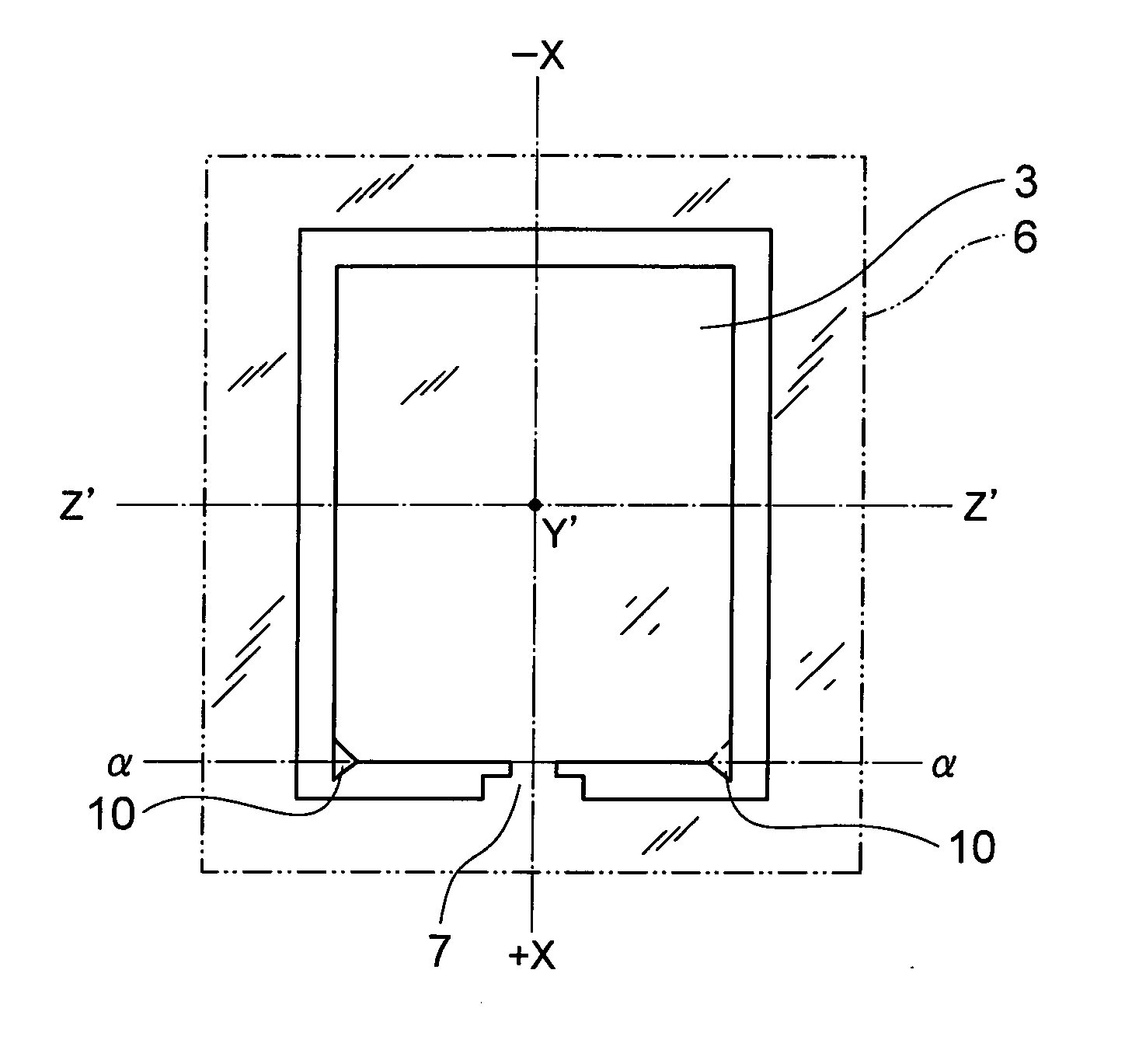
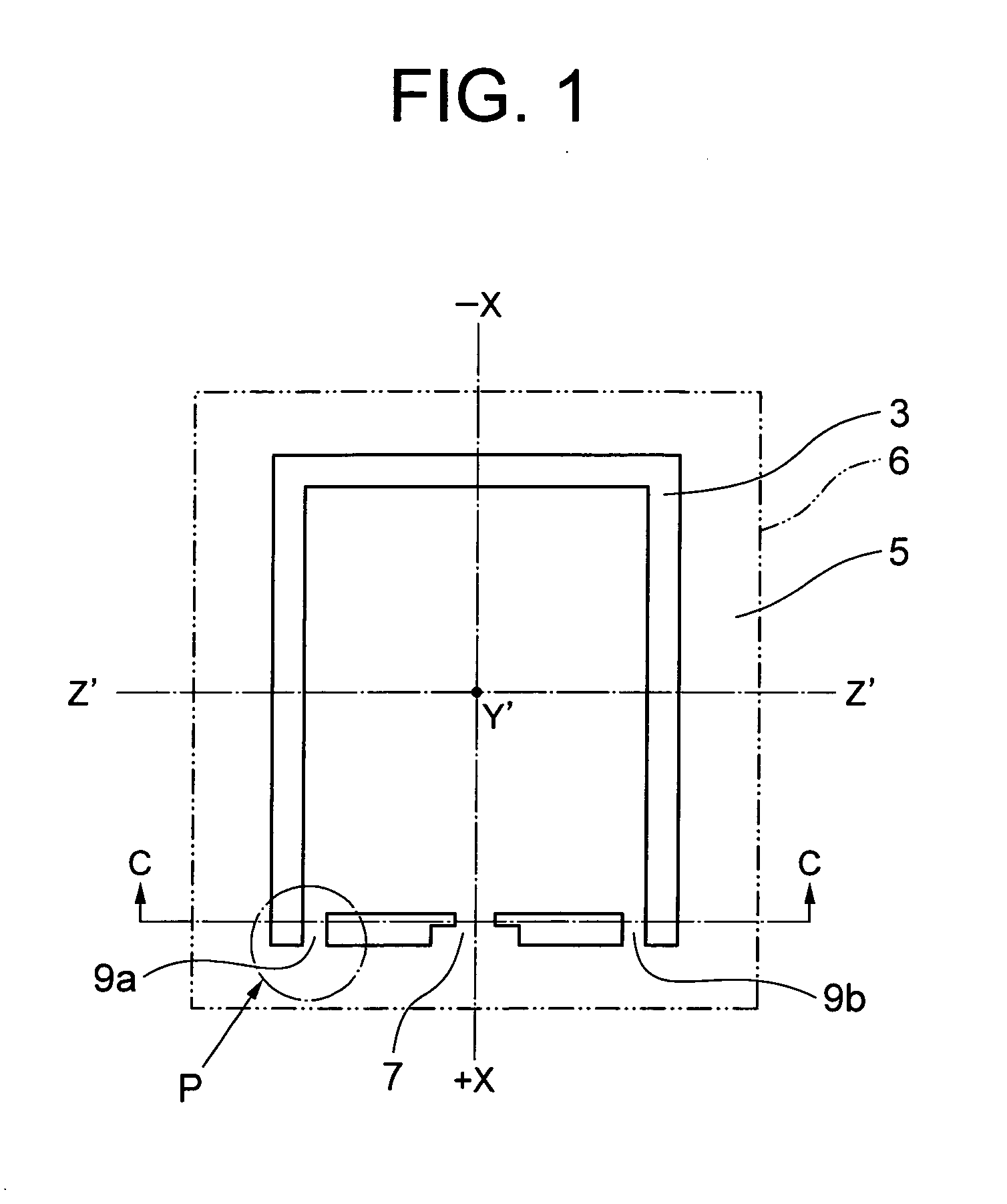
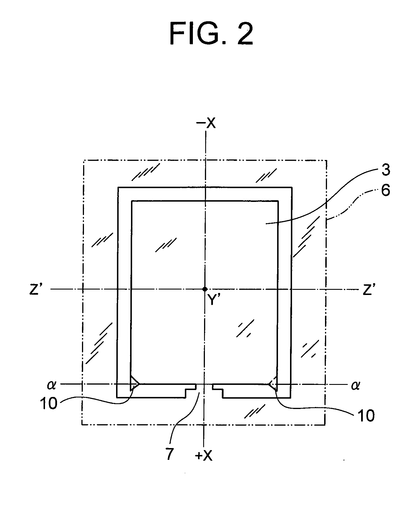
[0036]Hereunder, one embodiment of a crystal resonator manufacturing method of the present invention is described, with reference to FIG. 1 to FIG. 4. The same reference numbers are given to portions the same as those in the aforementioned conventional example, and descriptions thereof are simplified or omitted.

[0037]As mentioned above, a crystal resonator (crystal element) is an AT-cut element in which the principle surface thereof is orthogonal to the Y′-axis of the coordinate axis

[0038](XY′Z′) rotated about the X-axis of the crystal axis (XYZ). Moreover a large number of crystal elements 3 with a processed outer shape including a lead-out electrode and exciting electrode, are obtained by conducting photoetching on a crystal wafer 4 (refer to FIG. 6 to FIG. 8). Having conducted the outer-shape processing of the crystal element, an exciting electrode and lead-out electrode (not shown in the drawings) are formed on the principle surface of the crystal element by means of photoetchin...


PUM

PropertyMeasurementUnit
frequencyaaaaaaaaaa
widthaaaaaaaaaa
anisotropyaaaaaaaaaa

Abstract

There is provided a crystal resonator (crystal element) in which the probability of chipping occurring in separation is small when there is one supporting section with respect to a frame section of a crystal wafer, and inclined surfaces due to the anisotropy of etching are eliminated. The present invention relates to a crystal resonator manufacturing method such that an AT-cut crystal wafer is etched, a large number of rectangular crystal elements are joined with frame sections by supporting sections, and the crystal elements are mechanically cut away from the frame sections. On both sides of the +X-axis one end section of the crystal element, at least the outer side surface has a planarly tapered projection having a triangular inclined surface with an apex in the −X-axis direction, and the tip end of the projection has processing traces of the etching in the +X-axis direction.

Description

BACKGROUND OF THE INVENTION[0001]1. Technical Field[0002]The present invention relates to a crystal resonator (crystal element) manufacturing method in which outer-shape processing is conducted on a crystal wafer, and in particular, to a crystal resonator manufacturing method in which the method of crystal cutting is an AT cut method and the influence of anisotropy of wet etching is eliminated.[0003]2. Background Art[0004]An AT-cut crystal resonator is a typical type of crystal resonator, and is used in a frequency band from approximately 2 to 100 MHz (fundamental wave) as a built-in frequency source in various types of electronic devices. In recent years, there is a demand for mass-producing / processing crystal elements from a crystal wafer using a photolithography technique and etching (photoetching) technique, in order to increase the productivity.PRIOR ART[0005]FIG. 6 to FIG. 8 are diagrams for describing a crystal element cutting method of a conventional example, wherein FIG. 6 ...

Claims


Application Information

Patent Timeline
Patent Type & Authority Applications(United States)
IPC IPC(8): H01L41/22H01L41/09H01L41/18H01L41/332H03H3/02H03H9/19
CPCH03H3/04H03H9/02023H03H9/0595H03H9/19
Inventor TAKAHASHI, TAKEHIRO
Owner NIHON DEMPA KOGYO CO LTD
Why Eureka
Try Eureka