Imprint apparatus and method of manufacturing article
a technology of printing apparatus and manufacturing article, which is applied in the field of printing apparatus, can solve the problems of affecting the precision of a transfer pattern, destroying the concave-convex pattern of the mold, and posing a problem
- Summary
- Abstract
- Description
- Claims
- Application Information
AI Technical Summary
Benefits of technology
Problems solved by technology
Method used
Image
Examples
first embodiment
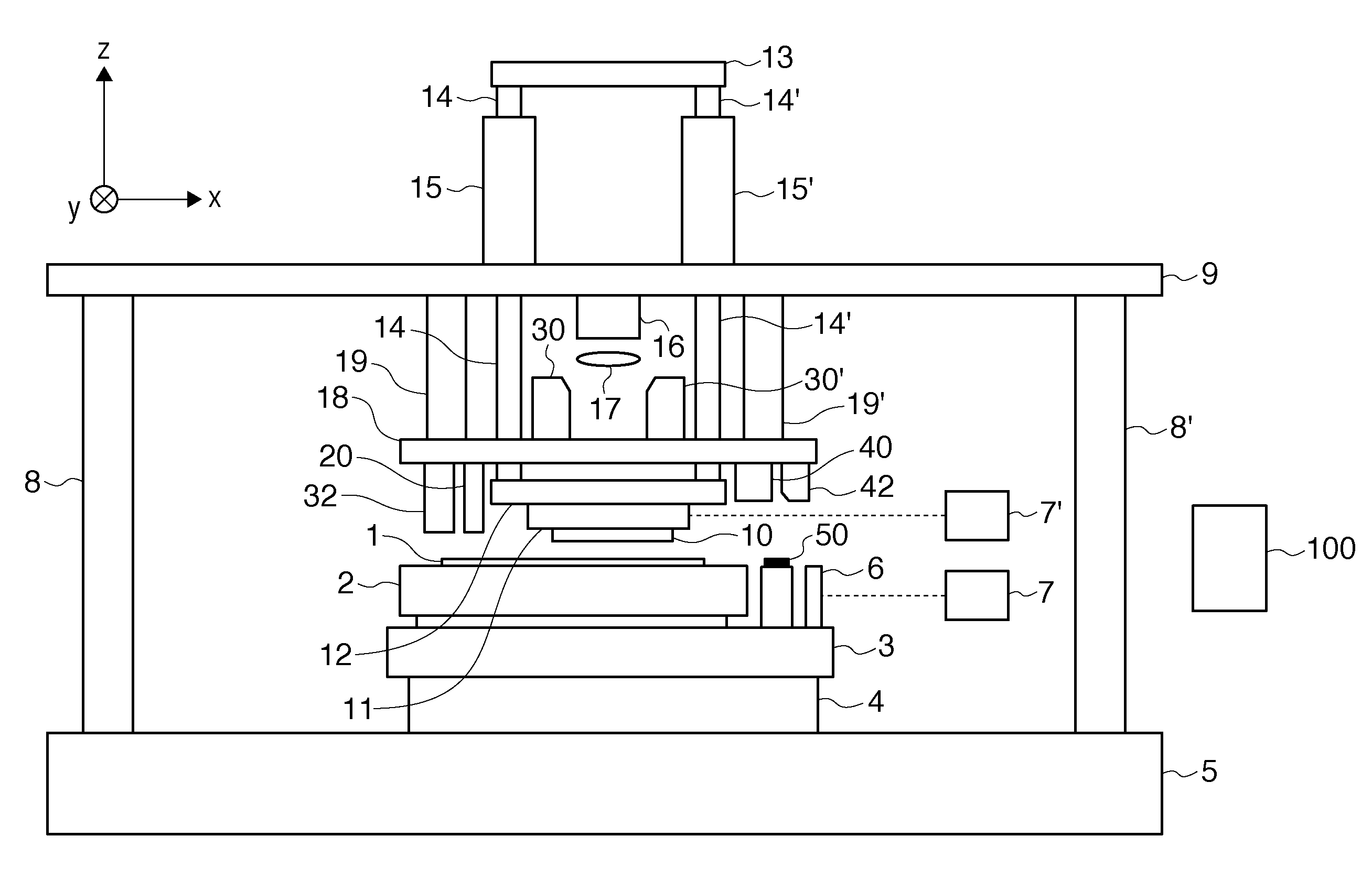
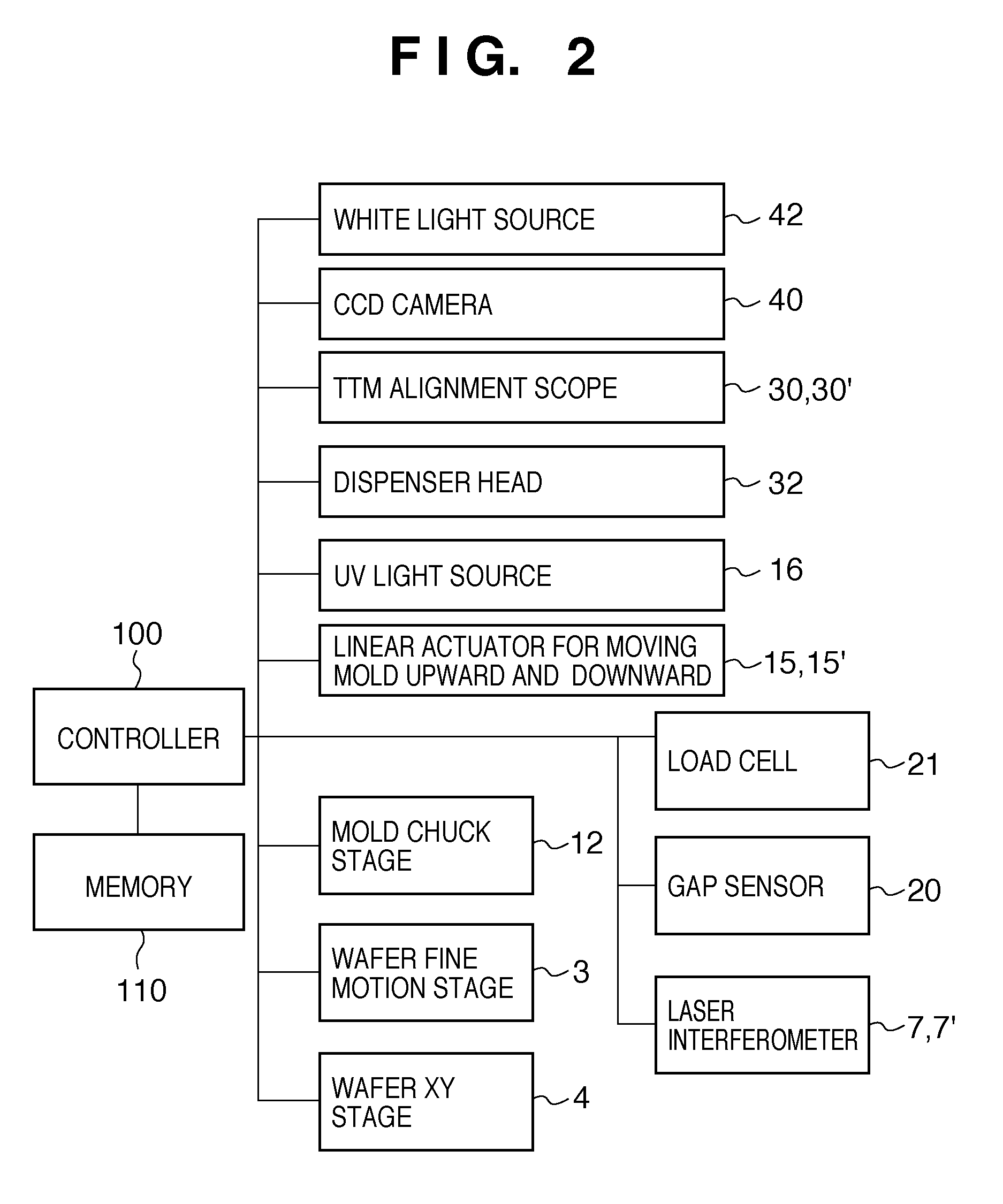
[0020]FIG. 1 is a view showing the arrangement of an imprint apparatus according to the first embodiment, and FIG. 2 is a control block diagram of the imprint apparatus according to respective embodiments. A wafer 1 as a substrate is held on a substrate chuck (wafer chuck) 2. A fine motion stage 3 has a correction function of a position in a θ (rotation about a z-axis) direction of the wafer 1, an adjustment function of a z-position of the wafer 1, and a tilt function of correcting a tilt of the wafer 1. The fine motion stage 3 is laid out on an XY stage 4 used to align the wafer 1 to a predetermined position. A combination of the fine motion stage 3 and XY stage 4 will be generally referred to as a substrate stage (wafer stage) hereinafter. The XY stage 4 is placed on a base surface plate 5. In order to measure the position of the fine motion stage 3, a reference mirror 6 which reflects light coming from a laser interferometer 7 is attached on the fine motion stage 3 to face in x- ...
second embodiment
[0033]The operation, functions, and the like of an imprint apparatus according to the second embodiment will be described below with reference to FIG. 7. The same reference numerals in FIG. 7 denote components having the same functions as in FIG. 1, and a description thereof will not be repeated. Referring to FIG. 7, reference numeral 41 denotes a beam splitter, which is arranged in an optical path from a UV light source 16, and guides reflected light coming from the side of a wafer 1 via a mold 10 toward a CCD camera 40 by bending the light. For the sake of simplicity, FIG. 7 does not illustrate one TTM alignment scope 30′. A flowchart of a process for transferring a pattern of certain layer onto a plurality of wafers using a single mold is the same as FIG. 3. FIG. 8 is a flowchart of a process for transferring a pattern on a single wafer using the imprint apparatus of the second embodiment, and corresponds to step S7 in FIG. 3. The same step numbers in FIG. 8 denote the steps of p...
PUM
| Property | Measurement | Unit |
|---|---|---|
| wavelength range | aaaaa | aaaaa |
| transparent | aaaaa | aaaaa |
| temperature | aaaaa | aaaaa |
Abstract
Description
Claims
Application Information


