Packaging substrate and fabrication method thereof

Active Publication Date: 2010-12-23
UNIMICRON TECH CORP
View PDF5 Cites 36 Cited by
  • Summary
  • Abstract
  • Description
  • Claims
  • Application Information

AI Technical Summary

Benefits of technology

[0031]Therefore, the present invention involves stacking two metal layers together, encapsulating the two metal layers with assistant dielectric layers, forming built-up structures on the assistant dielectric layers, and finally separating the built-up structures along the interface between the two metal layers so as to form two packaging substrates. Owing to the adhesive characteristic of the assistant dielectric layers, the two metal layers are unlikely to separate from each other during the formation of the built-up structures. But after the portions of the assistant dielectric layers around the periphery of the two metal layers are cut and removed, the two metal layers can be readily separated from each other. The two metal layers c

Problems solved by technology

However, the use of the core board increases the length of wires and thickness of the overall structure.
However, in the above method, the carrier board 10 and the thin metal layer 11 required for temporarily supporting the structure complic

Method used


Image

  • Packaging substrate and fabrication method thereof
  • Packaging substrate and fabrication method thereof
  • Packaging substrate and fabrication method thereof

Examples


Example

First Embodiment

[0039]FIGS. 2A to 2F are sectional views showing a packaging substrate and a method for fabricating the same according to a first embodiment of the present invention.

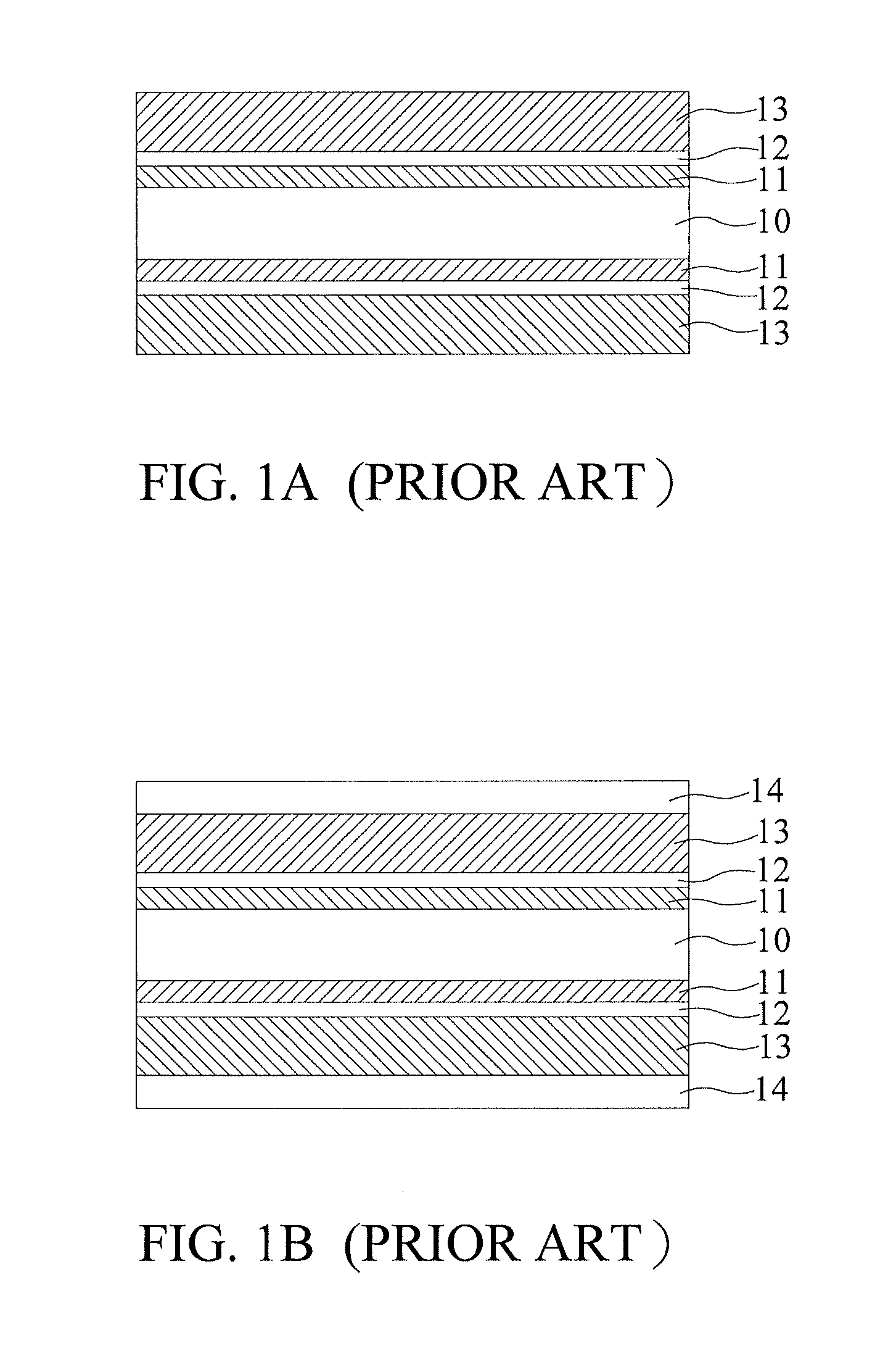
[0040]Referring to FIG. 2A, two first metal layers 20a, 20b respectively having first surfaces 201a, 201b and opposite second surfaces 202a, 202b are stacked together with the first surfaces 201a, 201b thereof facing each other; two first assistant dielectric layers 21a, 21b are formed on the second surfaces 202a, 202b of the first metal layers 20a, 20b, respectively; and two second metal layers 22a, 22b are formed on the exposed surfaces of the first assistant dielectric layers 21a, 21b, respectively, which can have a thickness greater than the thickness of the first metal layers 20a, 20b so as to provide sufficient rigidity.

[0041]In the present embodiment, the first surfaces 201a, 201b are smooth surfaces, and the second surfaces 202a, 202b are rough surfaces.

[0042]Referring to FIG. 2B, the first metal...

Example

Second Embodiment

[0050]FIGS. 3A to 3D are sectional views showing a packaging substrate and a method for fabricating the same according to a second embodiment of the present invention.

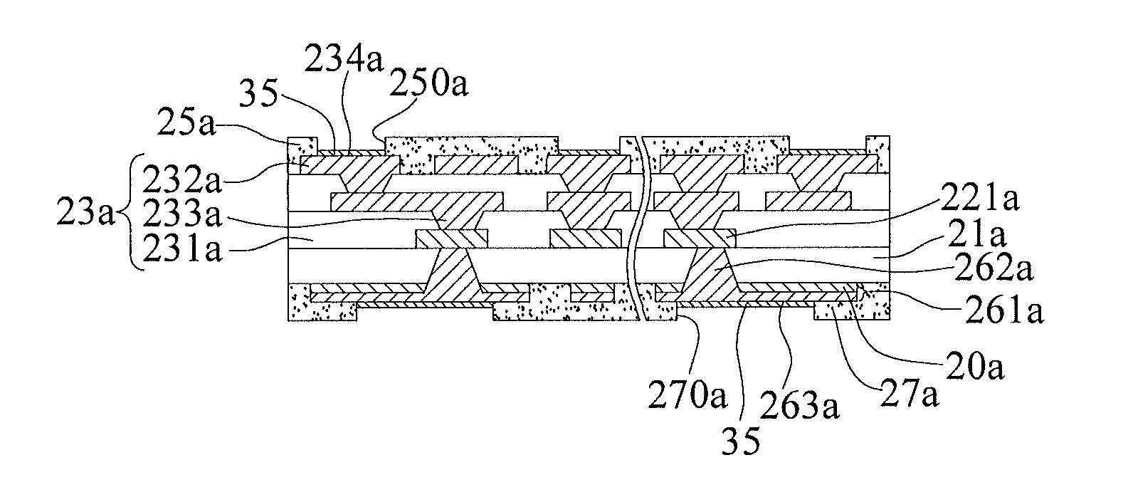
[0051]Referring to FIG. 3A, a structure as shown in FIG. 2C is obtained, the first wiring layers 232a, 232b disposed on an outermost portion of the built-up structures 23a, 23b have a plurality of first conductive pads 234a, 234b, respectively. First insulating protective layers 25a, 25b, such as solder mask layers, are formed on the outmost layers of the built-up structures 23a, 23b. A plurality of openings 250a, 250b corresponding in position to the first conductive pads 234a, 234b, respectively, are formed in the first insulating protective layers 25a, 25b so as for the first conductive pads 234a, 234b to be exposed from the first insulating protective layers 25a, 25b.

[0052]Referring to FIG. 3B, the overall structure is cut along cutting edges 24 passing through the first metal layers 20a, 20b.

[00...

Example

Third Embodiment

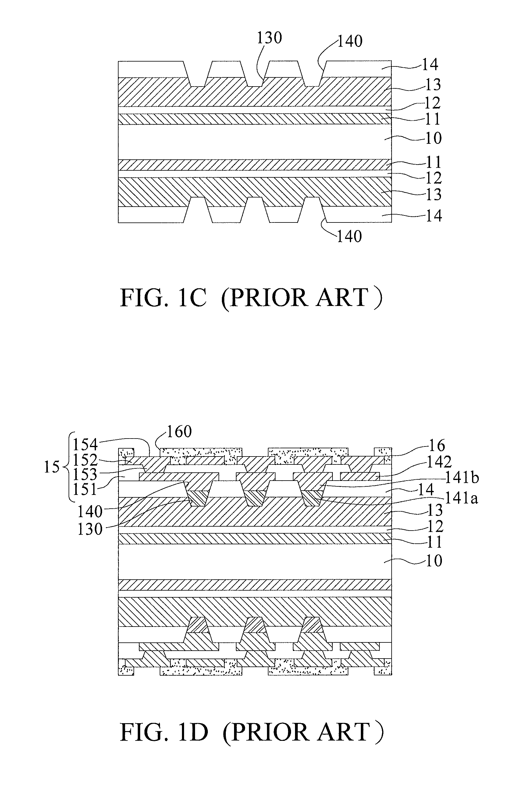
[0055]FIGS. 4A to 4F are sectional views showing a packaging substrate and a method for fabricating the same according to a third embodiment of the present invention, wherein FIGS. 4E′ and 4F′ show another embodiment of FIGS. 4E and 4F.

[0056]Referring to FIG. 4A, a structure as shown in FIG. 2B is obtained, and the second metal layers 22a, 22b are patterned so as to form inner wiring layers 301a, 301b. A plurality of inner conductive vias 302a, 302b are formed in the first assistant dielectric layers 21a, 21b to electrically connect the inner wiring layers 301a, 301b and the first metal layers 20a, 20b. The built-up structures 23a, 23b are formed on the first assistant dielectric layers 21a, 21b and inner wiring layers 301a, 301b. The built-up structures 23a, 23b at least comprise first dielectric layers 231a, 231b, first wiring layers 232a, 232b formed on the first dielectric layers 231a, 231b, and a plurality of first conductive vias 233a, 233b formed in the first ...


PUM

PropertyMeasurementUnit
Timeaaaaaaaaaa
Electrical conductoraaaaaaaaaa

Abstract

A method for fabricating a packaging substrate includes: stacking two metal layers; encapsulating the two metal layers with assistant dielectric layers; forming built-up structures on the assistant dielectric layers, respectively; and separating the built-up structures along the interface between the two metal layers so as to form two packaging substrates. Owing to the adhesive characteristic of the assistant dielectric layers, the two metal layers are unlikely to separate from each other during formation of the built-up structures. But after portions of the dielectric layer around the periphery of the metal layers are cut and removed, the two metal layers can be readily separated from each other. The two metal layers can be patterned to form wiring layers, metal bumps, or supporting structures to avoid waste of materials. A packaging substrate and a fabrication method thereof are provided.

Description

BACKGROUND OF THE INVENTION[0001]1. Field of the Invention[0002]The present invention relates generally to packaging substrates, fabrication methods thereof and base materials, and more particularly, to a low-cost packaging substrate and a fabrication method thereof.[0003]2. Description of Related Art[0004]Along with the development of electronic industries, electronic products have a trend towards miniaturization and high performance, and accordingly multi-layer boards are developed so as to increase the layout area for the layout through interlayer connection techniques, meet demands for high-density integrated circuits, and reduce the thickness of packaging substrates.[0005]Conventionally, a multi-layer board comprises a core board and built-up structures formed on two sides of the core board. However, the use of the core board increases the length of wires and thickness of the overall structure. Accordingly, coreless boards are developed to shorten the length of wires and reduce...

Claims


Application Information

Patent Timeline
IPC IPC(8): H05K1/03B32B37/00B32B38/10H05K1/11
CPCH05K3/0097H01L2224/48227H05K2203/0152H05K2203/1536H05K13/00Y10T156/10H05K3/4682H01L2224/48091H01L2224/32225H01L2224/16225H01L2224/73204H01L2924/15311H01L2924/15174H01L2224/73265H01L2924/00014H01L2924/00H01L2224/05573H01L2224/05568H01L2224/0554H01L2224/05599H01L2224/0555H01L2224/0556
Inventor LIU, CHIN-MING
Owner UNIMICRON TECH CORP
Why Eureka
Try Eureka