

Method for manufacturing semiconductor device
- Summary
- Abstract
- Description
- Claims
- Application Information
AI Technical Summary
Benefits of technology
Problems solved by technology
Method used
Image

Examples
embodiment
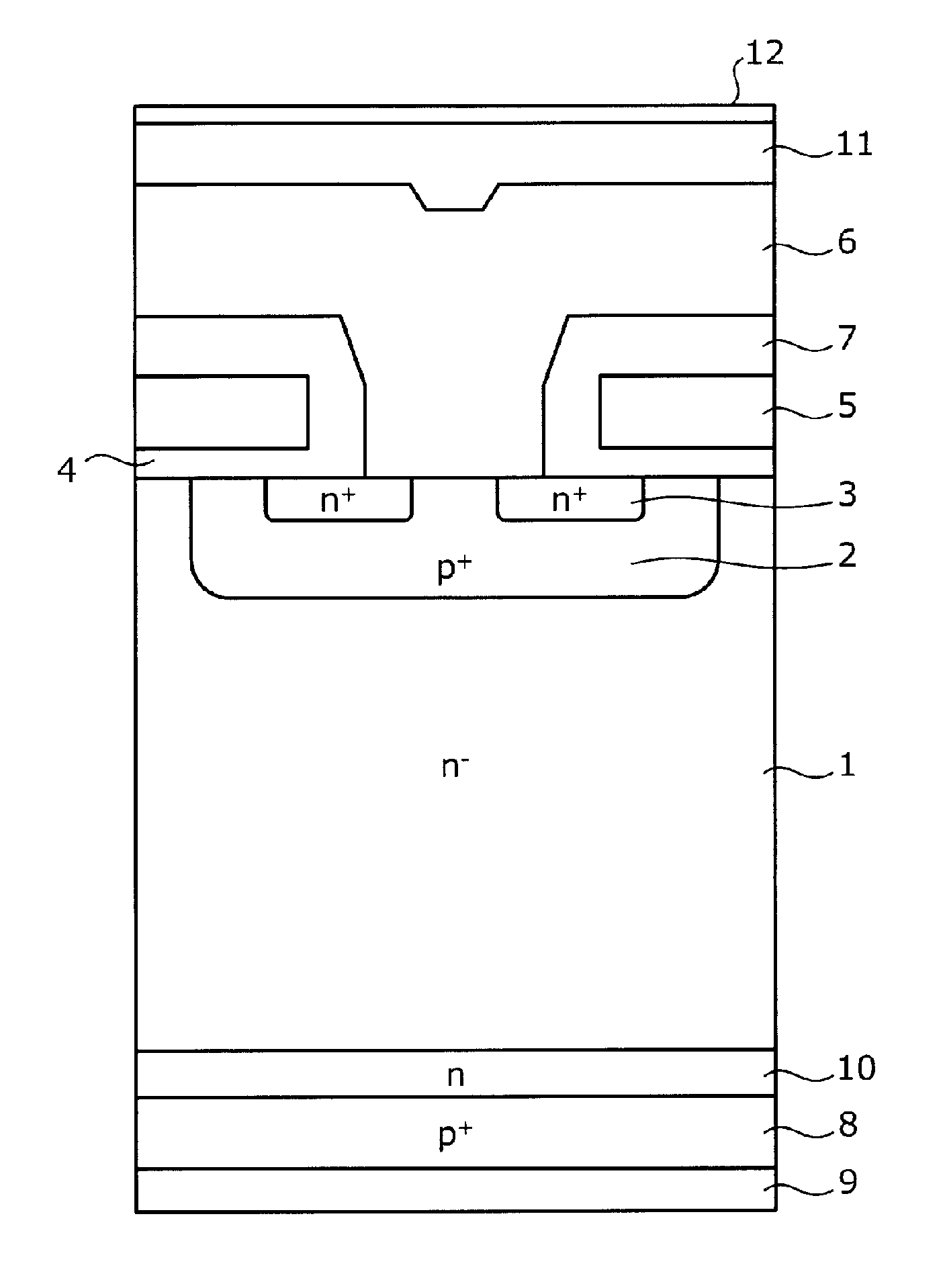
[0060]Firstly, a semiconductor device which is manufactured by the method for manufacturing a semiconductor device according to an embodiment will be described, taking as an example a field stop (FS)-type IGBT having a planar gate structure. FIG. 1 is a cross-sectional diagram showing the configuration of a semiconductor device manufactured by the method for manufacturing a semiconductor device according to this embodiment. As shown in FIG. 1, the semiconductor device according to the present invention has a front surface element structure in which, for example, an n− type semiconductor substrate (FZ substrate) manufactured by a floating zone method is used as an n− type drift layer 1, and a MOS gate (insulated gate comprising metal-oxide film-semiconductor) structure is formed on one main surface (front surface) side thereof. The n− type drift layer 1 has the function of an active layer. The MOS gate structure includes a p+ type base region 2, an n+ type emitter region 3, a gate in...
first example
[0104]Next, the relationship between the Shore hardness and the durability of the pressing roller 41 was investigated. FIG. 13 is a characteristics diagram showing a relationship between the Shore hardness and durability of the pressing roller. A plurality of semiconductor devices (called “First Example” below) was formed using pressing rollers 41 having different Shore hardnesses, in accordance with the semiconductor device according to the embodiment described above. In each of the First Examples, a plurality of samples is manufactured using 1000 semiconductor wafers 20 each time. The diameter and product thickness of the semiconductor wafer 20 were 8 inches and 80 μm respectively. The pressing pressure of the pressing roller 41 and the angle θ of the V groove 41a were respectively 150 kPa and 120 degrees. The sandwiching roller 42 was a one-stage roller. In each of the samples in the First Example, the state of the semiconductor wafer 20 and the second film 22 after the plating p...
second example
[0107]Next, the relationship between the pressing pressure and the durability of the pressing roller 41 was investigated. FIG. 14 is a characteristics diagram showing a relationship between the pressing pressure and durability of the pressing roller. A plurality of semiconductor devices (called “Second Example” below) was formed by variously altering the pressing pressure of the pressing roller 41 when bonding the second film 22, in accordance with the semiconductor device according to the embodiment described above. In each of the Second Examples, a plurality of samples was manufactured using 1000 semiconductor wafers 20 each time. The diameter and product thickness of the semiconductor wafer 20 were similar to the First Example. The Shore hardness of the pressing roller 41 and the angle θ of the V groove 41a were respectively 60 degrees and 120 degrees. The sandwiching roller 42 was a one-stage roller. The state after the plating process and the state of the pressing roller 41 wer...
PUM
 Abstract
Description
Claims
Application Information