

Method for forming a self aligned isolation trench
- Summary
- Abstract
- Description
- Claims
- Application Information
AI Technical Summary
Benefits of technology
Problems solved by technology
Method used
Image

Examples
Embodiment Construction
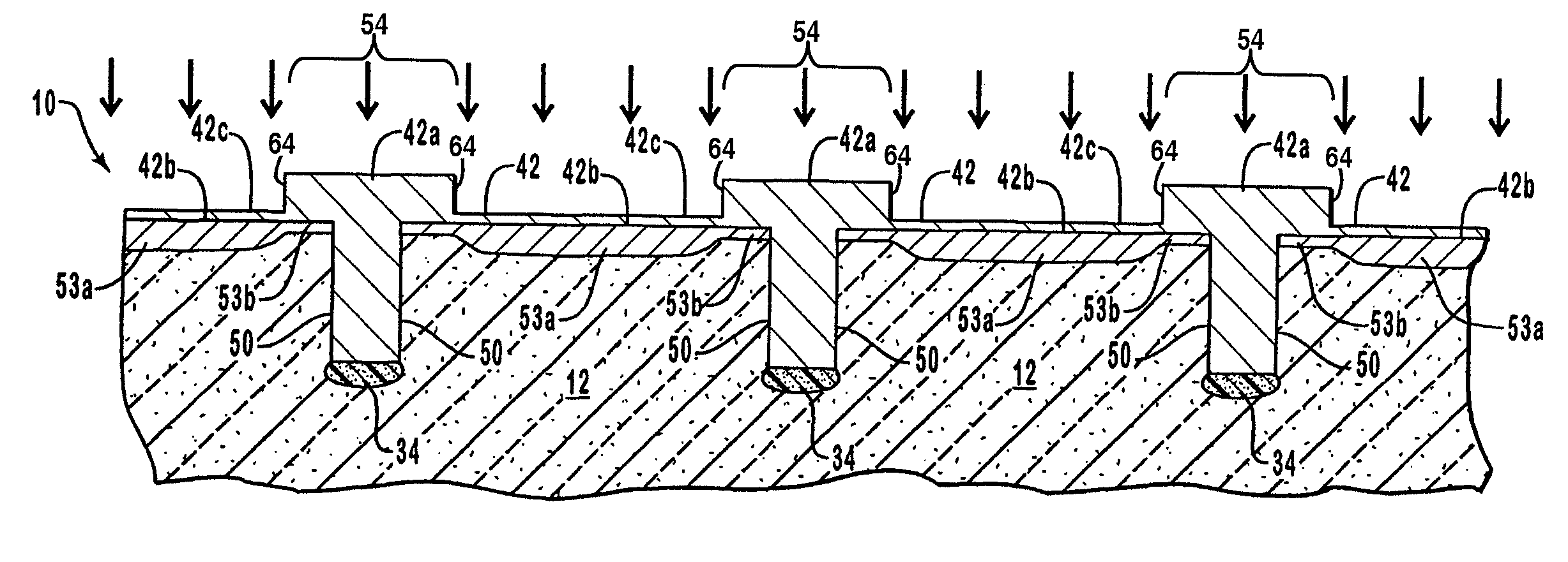
[0030]The present invention relates to a method for forming a self-aligned isolation trench. The isolation trench is preferably a shallow trench isolation region that is self-aligned to an underlying active area. Stated otherwise, the inventive method forms a Narrow self-aligned Active area Isolation region that is inherently Level (NAIL). In the method of the present invention, a spacer etch and an isolation trench etch can be accomplished essentially within the same processing step.
[0031]Another aspect of the present invention relates to a combined nitride and oxide etch that is selective to polysilicon, and in which selectivity of the etch between nitride and oxide materials favors one or the other by a factor of about one half. A still further aspect of the present invention relates to the use of a polysilicon film as an etch stop or planarization marker film. The structure achieved by the method of the present invention achieves particular advantages that overcome problems of t...
PUM
 Abstract
Description
Claims
Application Information