

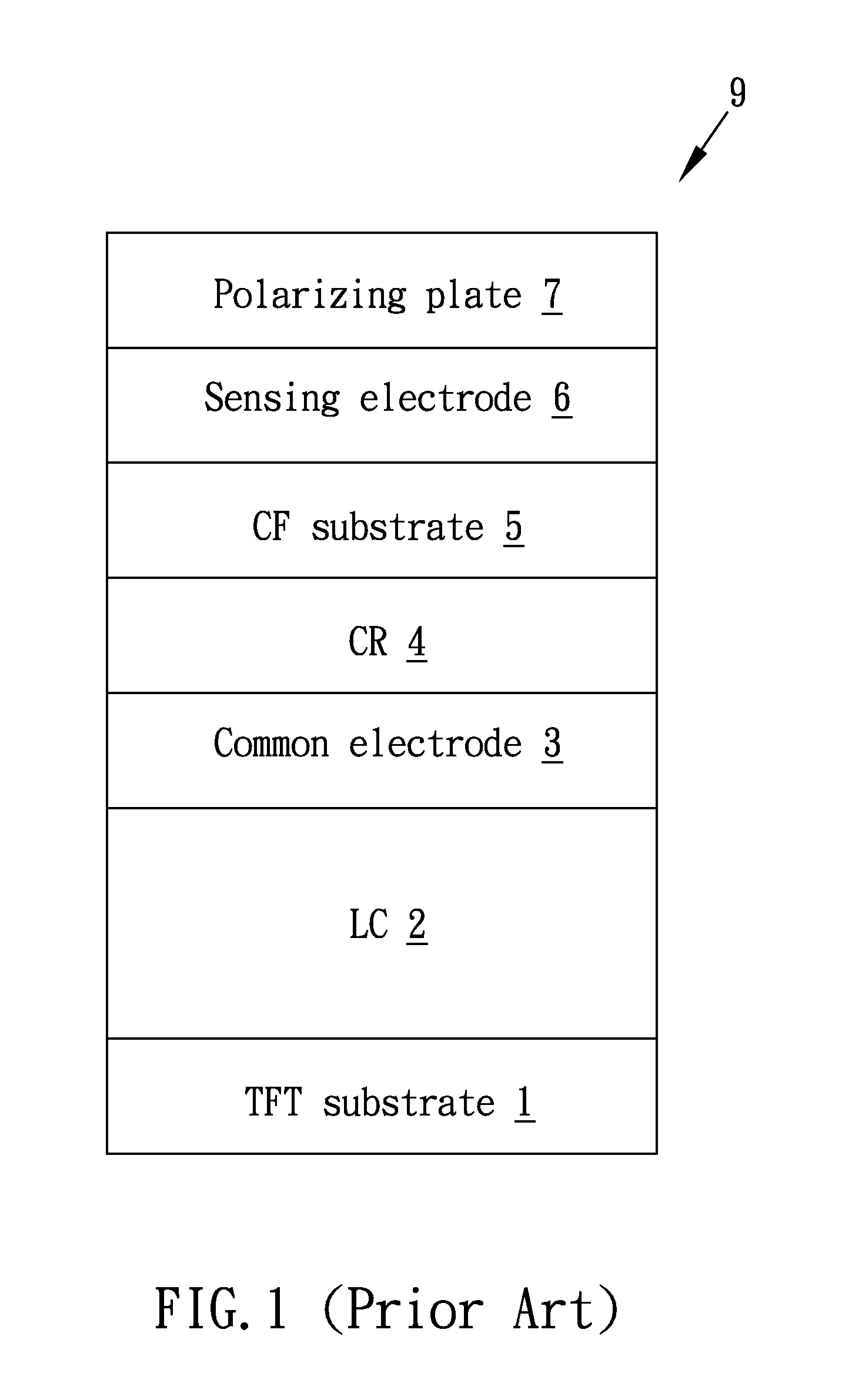
Touch sensitive ips liquid crystal display
a liquid crystal display and touch sensitive technology, applied in the field of touch panels, can solve the problems affecting the touch performance and accuracy of the sensing electrode layer, and achieve the effects of reducing the electric field effect, improving the sensing performance and accuracy, and high background capacitan
- Summary
- Abstract
- Description
- Claims
- Application Information
AI Technical Summary
Benefits of technology
Problems solved by technology
Method used
Image

Examples
first embodiment
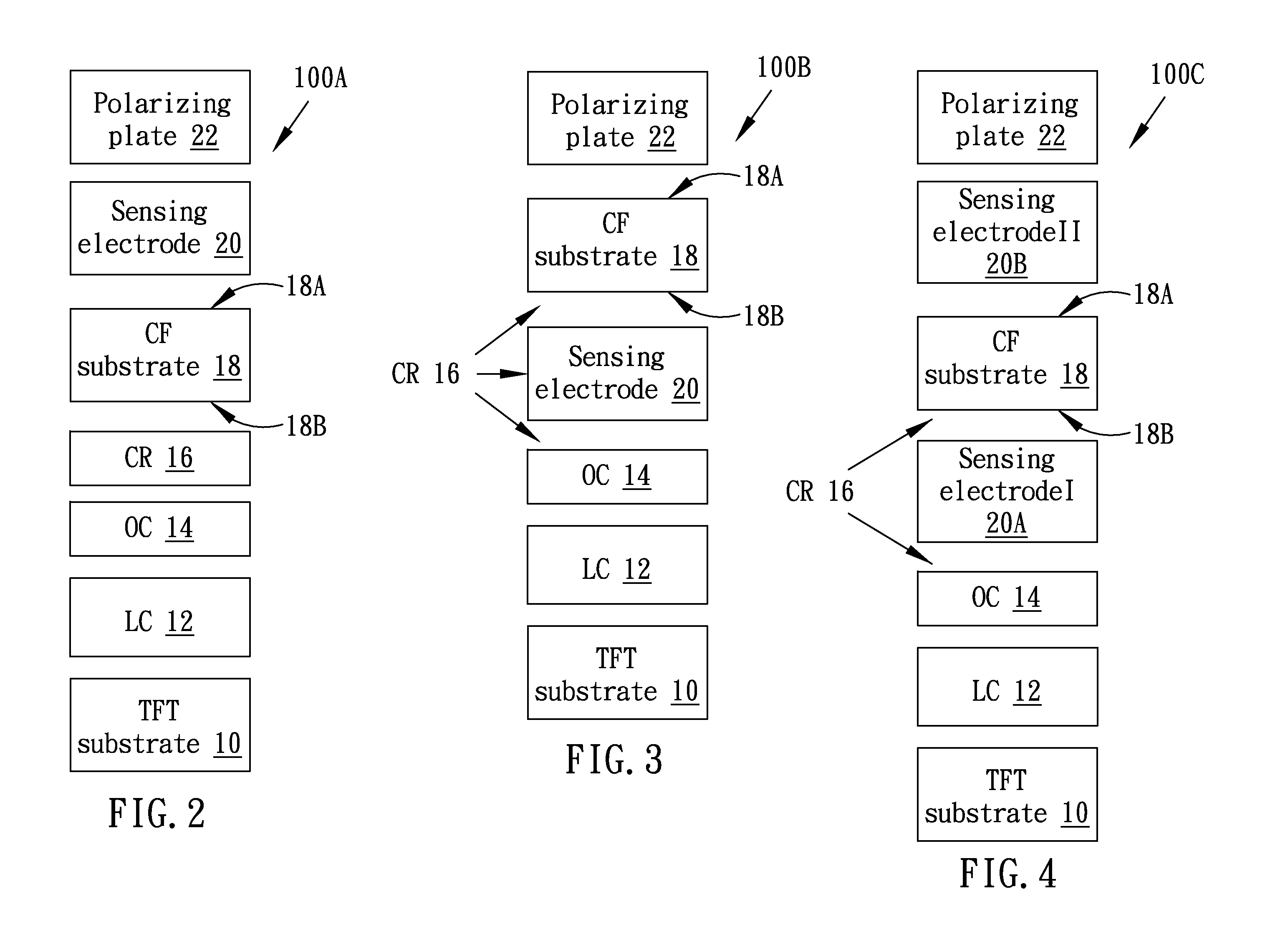
[0028]FIG. 2 is a cross-sectional view of a touch sensitive in-plane switching (IPS) liquid crystal display (LCD) 100A, abbreviated as the touch sensitive display hereinafter, according to the present invention. Terms such as “above” / “below” and “top” / “bottom” in this specification are used to represent relative directions. With respect to the figures accompanying this description, tops and bottoms of the depicted touch sensitive displays appear nearer to and further from the viewer respectively. Capacitive sensing is utilized in the embodiments of the present invention to detect touch positions according to capacitance variations at the touch points of a user's finger or stylus.
[0029]The structure and display mode of the touch sensitive display according to the present embodiments implement IPS, which is distinct from other display modes owing at least to the following differences. Both the common electrode layer and the pixel electrode of the IPS LCD are disposed below the liquid ...
second embodiment
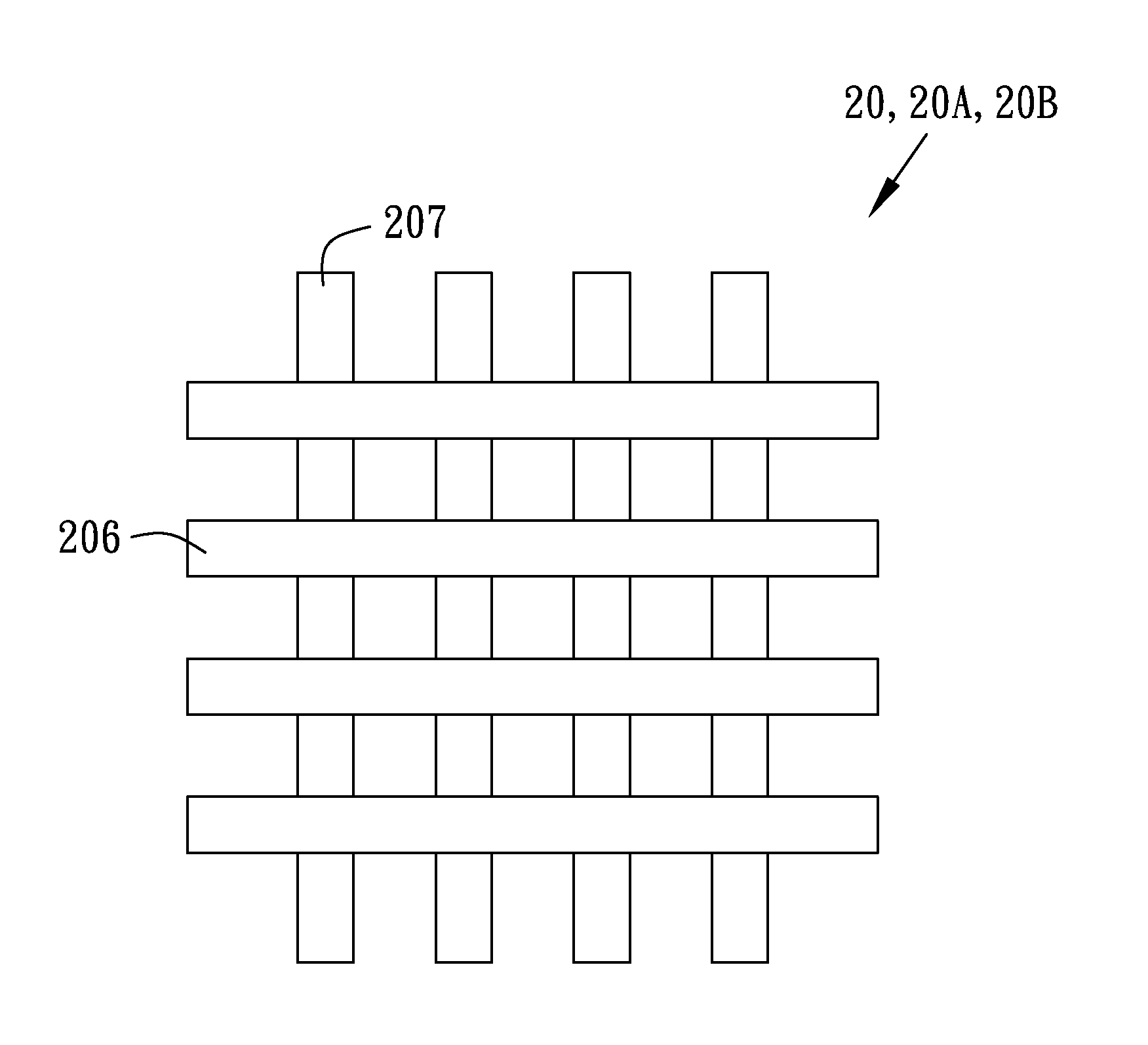
[0032]FIG. 3 is a cross-sectional view of a touch sensitive IPS LCD 100B according to the present invention. In the embodiment, the touch sensitive display 100B includes, from bottom to top, an active-matrix transistor (such as TFT) substrate 10, an LC layer 12, an OC layer 14, a sensing electrode layer 20, a CF substrate 18, and a polarizing plate 22. A CR layer 16 may be disposed between the OC layer 14 and the sensing electrode layer 20; or may be disposed between the sensing electrode 20 and the CF substrate 18; or may even be disposed in the sensing electrode layer 20, as indicated by the arrows. An additional layer or layers may be inserted between the aforementioned composing layers according to particular applications or functions.
[0033]One aspect of the second embodiment (FIG. 3) is that, with respect to structure, the sensing electrode layer 20 is disposed between the CF substrate 18 and the OC layer 14, or, in other words, below the CF substrate 18. Specifically, the sens...
third embodiment
[0034]FIG. 4 is a cross-sectional view of a touch sensitive IPS LCD 100C according to the present invention. In the embodiment, the touch sensitive display 100C includes, from bottom to top, an active-matrix transistor (such as TFT) substrate 10, an LC layer 12, an OC layer 14, a first (I) sensing electrode layer 20A, a CF substrate 18, a second (II) sensing electrode layer 20B, and a polarizing plate 22. A CR layer 16 may be disposed between the OC layer 14 and the first sensing electrode layer 20A; or may be disposed between the first sensing electrode 20A and the CF substrate 18, as indicated by the arrows. An additional layer or layers may be inserted between the aforementioned composing layers according to the particular application or function.
[0035]One aspect of the third embodiment (FIG. 4) is that, with respect to structure, the sensing electrode layer is divided into two parts: the first sensing electrode layer 20A and the second sensing electrode layer 20B, which are disp...
PUM
 Abstract
Description
Claims
Application Information