Power module with additional transient current path and power module system

Inactive Publication Date: 2010-12-30
VINCOTECH HLDG R L
View PDF6 Cites 33 Cited by
  • Summary
  • Abstract
  • Description
  • Claims
  • Application Information

AI Technical Summary

Benefits of technology

[0011]For instance, the transient current path can at least partly be formed as a sandwich of at least two electrically conductive sheets, preferably fabricated from stamped and bent metal sheets. This is a particularly easy and cost efficient way of fabricating a contact bridge with int

Problems solved by technology

Generally, parasitic inductances are a major problem with such power modules, in particular in fast switching applications.
The parasitic inductance causes overvoltages and increases switch-off losses in the semiconductor.
In particular, when using an insulated gate bipolar transistor (IGBT), the switchi

Method used


Image

  • Power module with additional transient current path and power module system
  • Power module with additional transient current path and power module system
  • Power module with additional transient current path and power module system

Examples


Example

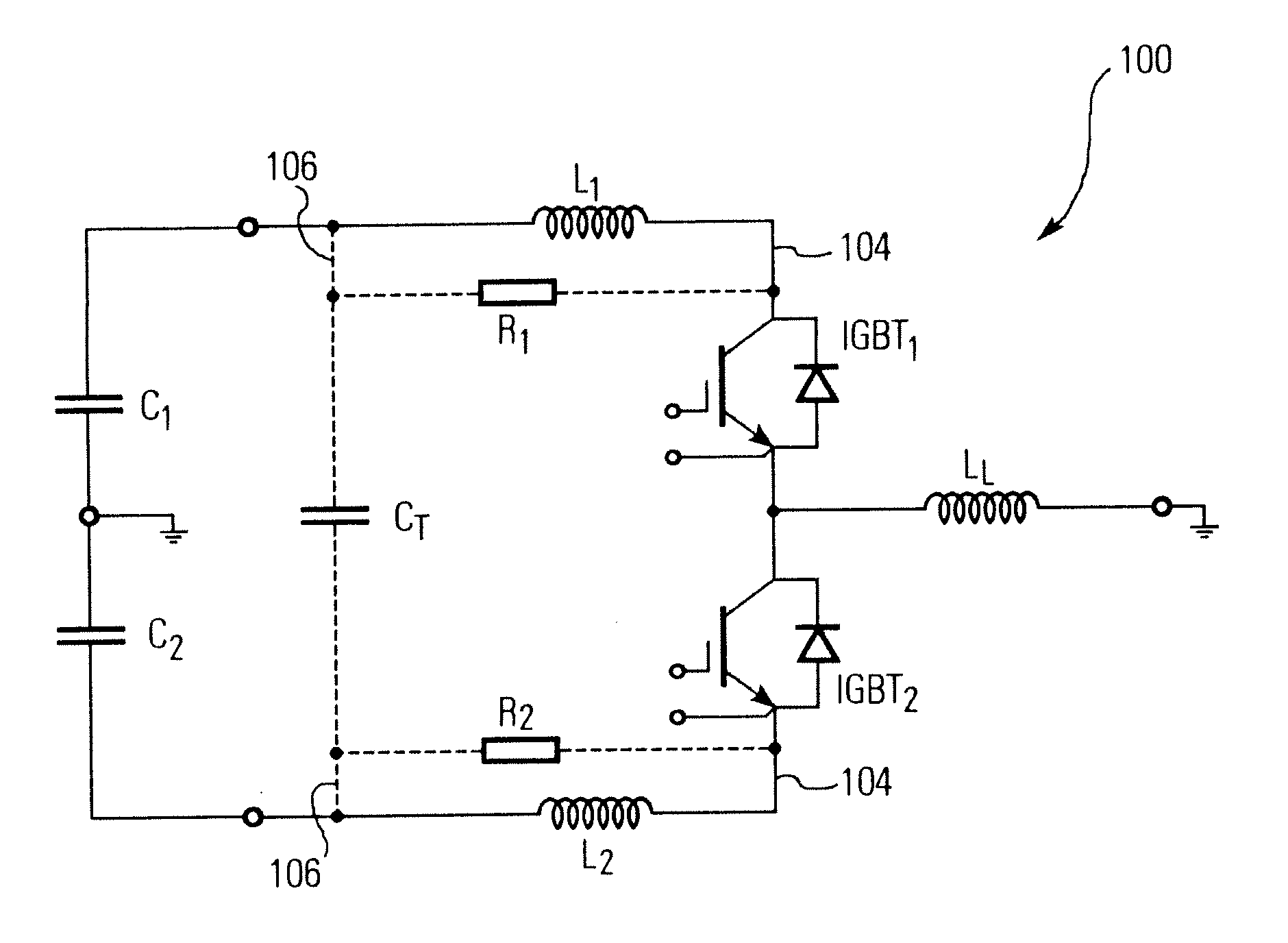
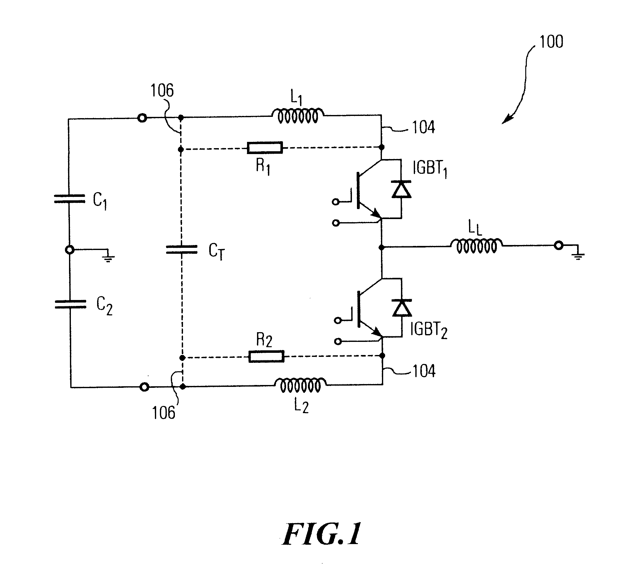
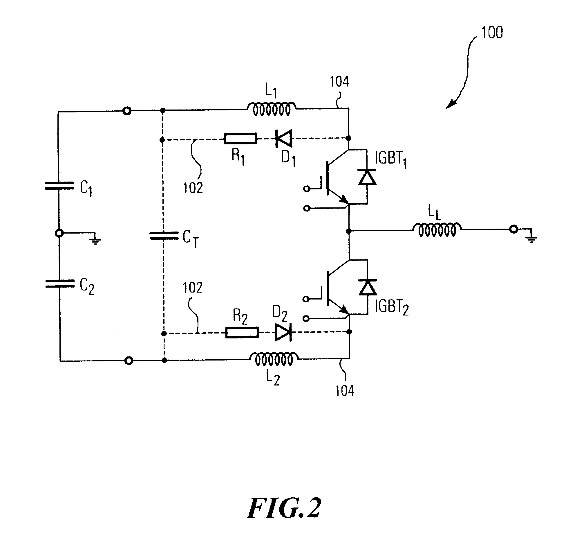
[0023]FIG. 1 shows a schematic circuit diagram of a power module 100 according to the present invention in a first embodiment. The power module 100 is structured as a half bridge comprising two insulated gate bipolar transistors, IGBT, connecting a DC input to a load LL. According to the present invention, the current flow in the power module 100 is separated into a transient path 102 with extremely low inductivity for the transient current during switching the high voltage and a main path 104 having a low resistance for the continuous current. The discrete elements L1, R1 and L2, R2 represent the distributed parasitic inductivities and resistances of the respective current paths. As shown in FIG. 1, the main current path 104 does not have a significant ohmic resistance, but only a measurable inductivity L1 and L2.

[0024]On the other hand, the inventive transient current path 102 exhibits a measurable ohmic resistance R1, R2, but is designed in a way that it is extremely low in induc...


PUM


Abstract

The present invention relates to power modules for controlling an input current to provide an output current, in particular, to such a power module (100) comprising at least one semiconductor switch for controlling the input current and a circuit substrate. The circuit substrate (108, 110) has at least one input terminal for being connected to an input voltage and at least one output terminal for outputting the output voltage. The input terminal and the output terminal are connected to each other via a main current path (104) that is controlled by the semiconductor switch. Said power module further comprises at least one transient current path (102) with extremely low inductivity for carrying a transient current during a switching operation of the semiconductor switch. The main path for the continuous current has a low ohmic resistance, but does not have to be designed to have a specifically low inductance.

Description

BACKGROUND OF THE INVENTION[0001]The present invention relates to power modules for controlling an input current to provide an output current. In particular, the present invention relates to such a power module comprising at least one semiconductor switch for controlling the input current and a circuit substrate. The circuit substrate has at least one input terminal for being connected to an input voltage and at least one output terminal for outputting the output voltage. The input terminal and the output terminal are connected to each other via a main current path that is controlled by the semiconductor switch.[0002]Generally, parasitic inductances are a major problem with such power modules, in particular in fast switching applications. The parasitic inductance causes overvoltages and increases switch-off losses in the semiconductor. In particular, when using an insulated gate bipolar transistor (IGBT), the switching off of the semiconductor switch results in a current change and ...

Claims


Application Information

Patent Timeline
IPC IPC(8): H02H3/22
CPCH01L23/642H01L25/072H01L25/162H02M7/003H01L2924/0002H03K17/08148H01L2924/00H02M7/487
Inventor FRISCH, MICHAELTEMESI, ERNO
Owner VINCOTECH HLDG R L
Why Eureka
Try Eureka