Unlock instant, AI-driven research and patent intelligence for your innovation.

Delay locked loop circuit

Inactive Publication Date: 2011-01-06
SK HYNIX INC
View PDF4 Cites 10 Cited by
  • Summary
  • Abstract
  • Description
  • Claims
  • Application Information

AI Technical Summary

Benefits of technology

An embodiment of the present invention is directed to providing a delay locked loop circuit that can stably perform a delay locked operation regardless of a variation in the level of external power source voltage.

Problems solved by technology

The internal clock, however, becomes delayed as it goes through the constituent elements of the memory and when it is outputted from the memory, it is not synchronized with an external clock.
Since each delay cell is formed of an active device such as a NAND gate or an inverter, each delay cell may have a problem of a delay amount varying according to a change in the level of an external power source voltage VDD.

Method used


Image

  • Delay locked loop circuit
  • Delay locked loop circuit
  • Delay locked loop circuit

Examples


first embodiment

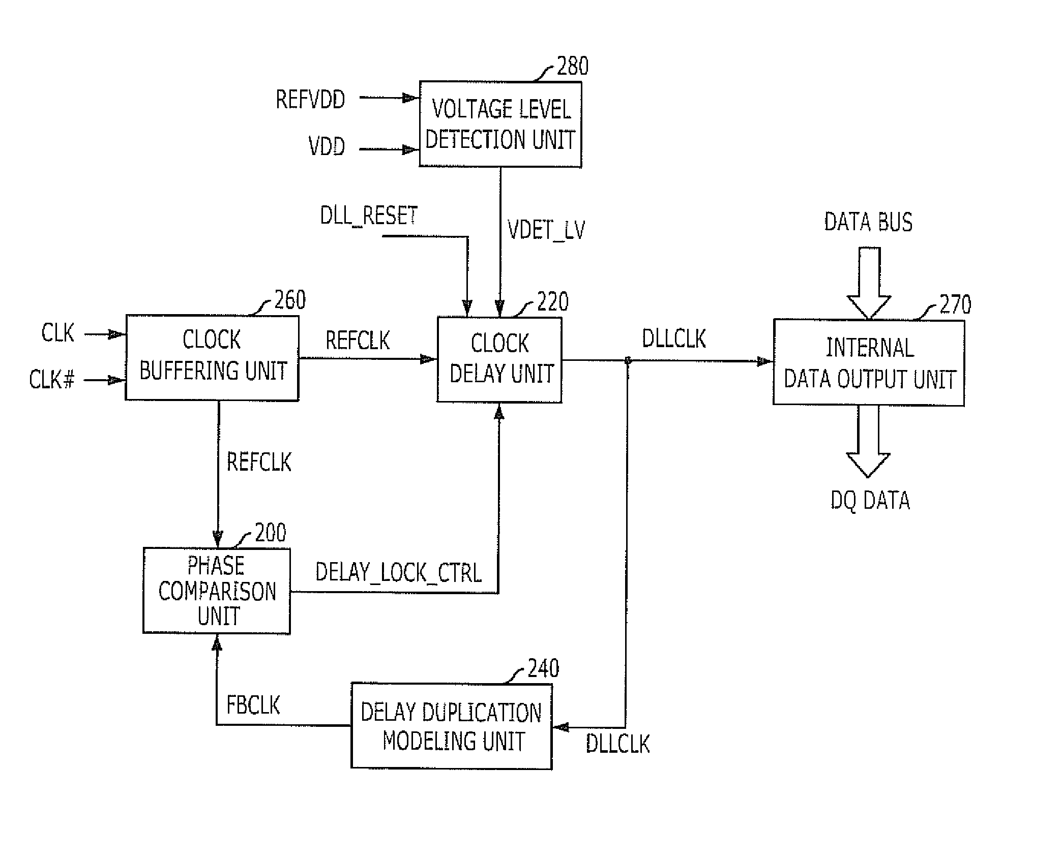
FIG. 2 is a block diagram illustrating a register-controlled delay locked loop circuit in accordance with the present invention.

FIG. 3 is a block diagram depicting a clock delay unit of the register-controlled delay locked loop circuit shown in FIG. 2 in accordance with the first embodiment of the present invention.

Referring to FIGS. 2 and 3, the register-controlled delay locked loop circuit includes a voltage level detection unit 280, a phase comparison unit 200, a clock delay unit 220, and a delay duplication modeling unit 240. The voltage level detection unit 280 detects the level of external power source voltage VDD. The phase comparison unit 200 compares the phase of a reference clock REFCLK with the phase of a feedback clock FBCLK.

The clock delay unit 220 designates any one of a delay time unit of a first delay cell SUD, which will be referred to as a first delay cell unit hereafter, and a delay time unit of a second delay cell LUD, which will be referred to as a second delay ...

second embodiment

FIG. 5 is a block diagram illustrating a register-controlled delay locked loop circuit in accordance with the present invention.

FIG. 6 is a block diagram depicting a clock delay unit in the register-controlled delay locked loop circuit shown in FIG. 5 in accordance with the second embodiment of the present invention.

Referring to FIGS. 5 and 6, the register-controlled delay locked loop circuit includes a voltage level detection unit 580, a phase comparison unit 500, a first clock delay unit 520, a second clock delay unit 530, a delay selection control unit 590, and a delay duplication modeling unit 540. The voltage level detection unit 580 detects the level of an external power source voltage VDD. The phase comparison unit 500 compares the phase of a feedback clock FBCLK with the phase of a reference clock REFCLK. The first clock delay unit 520 delays the reference clock REFCLK by a first delay cell unit in response to an output signal DELAY_LOCK_CTRL of the phase comparison unit 500...


PUM


Abstract

A delay locked loop circuit includes: a voltage level detector for detecting of an external power source voltage level; a phase comparator for comparing phases of reference clock and feedback clock; a clock delayer for designating one of a first delay cell unit and a second delay cell unit as initial delay cell unit and the other as connected delay cell unit, delaying the reference clock by the initial delay cell unit until delay amount of the reference clock reaches a predetermined delay amount, delaying the reference clock by the connected delay cell unit after the delay amount of the reference clock reaches the predetermined delay amount in response to an output signal of the phase comparator, and outputting a delay locked clock; and a delay duplication modeler for changing the delay locked clock to reflect an actual delay condition of the reference clock and outputting the feedback clock.

Description

CROSS-REFERENCE TO RELATED APPLICATIONSThe present application claims priority of Korean Patent Application No. 10-2009-0059712, filed on Jul. 1, 2009, which is incorporated herein by reference in its entirety.BACKGROUND OF THE INVENTIONExemplary embodiments of the present invention relate to semiconductor designing technology, and more particularly, to a delay locked loop circuit.A synchronous semiconductor memory device such as Double Data Rate Synchronous Dynamic Random Access Memory (DDR SDRAM) transfers / receives data to / from an external device by using an internal clock synchronized with an external clock inputted from the external device such as a memory controller. It is important to temporally synchronize a data outputted from a memory with an external clock supplied from a memory controller to the memory to stably transfer data between the memory and the memory controller.The data is outputted from the memory in synchronization with an internal clock. When the internal cloc...

Claims


Application Information

Patent Timeline
IPC IPC(8): H03L7/06
CPCG11C7/222H03L7/0816H03L7/0814H03L7/07G11C8/00G11C11/407
Inventor CHUNG, JIN-IL
Owner SK HYNIX INC
Features
  • R&D
  • Intellectual Property
  • Life Sciences
  • Materials
  • Tech Scout
  • Unparalleled Data Quality
  • Higher Quality Content
  • 60% Fewer Hallucinations
Learn More