Differential class ab amplifier circuit, driver circuit and display device

a technology of driver circuit and amplifier circuit, which is applied in the direction of different amplifiers, amplifiers with semiconductor devices/discharge tubes, instruments, etc., can solve the problems of parasitic capacitance on data lines, increased size, and low power consumption of driver circuits, and achieve the effect of improving phase margin

Inactive Publication Date: 2011-01-13
RENESAS ELECTRONICS CORP
View PDF1 Cites 11 Cited by
  • Summary
  • Abstract
  • Description
  • Claims
  • Application Information

AI Technical Summary

Benefits of technology

[0022]According to the present invention, the differential class AB amplifier circuit, the driver circuit and the display device which can improve a phase margin can be provided.

Problems solved by technology

Furthermore, a low power consumption is required to those driver circuits.
Meanwhile, a liquid crystal panel has increased in size and in result parasitic capacitances on the data lines have also increased.
Generally, in a case where a voltage follower connected two-stage differential amplifier circuit is used with an input circuit having a differential amplifier and an output circuit for amplifying a signal from the differential amplifier, its operation easily becomes unstable when load capacitances applied to the output increase.
In some cases, the circuit may oscillate.
However, the phase compensating circuit generally occupies a large area, and gives a great impact on an increase in chip area of the whole display device driver circuit having a large number of differential class AB amplifier circuits, thereby an increase in manufacturing costs is led.
Furthermore, the number of current paths between the power voltage sources VDD and VSS increases, resulting in an increase in power consumption.

Method used


Image

  • Differential class ab amplifier circuit, driver circuit and display device
  • Differential class ab amplifier circuit, driver circuit and display device
  • Differential class ab amplifier circuit, driver circuit and display device

Examples


Embodiment Construction

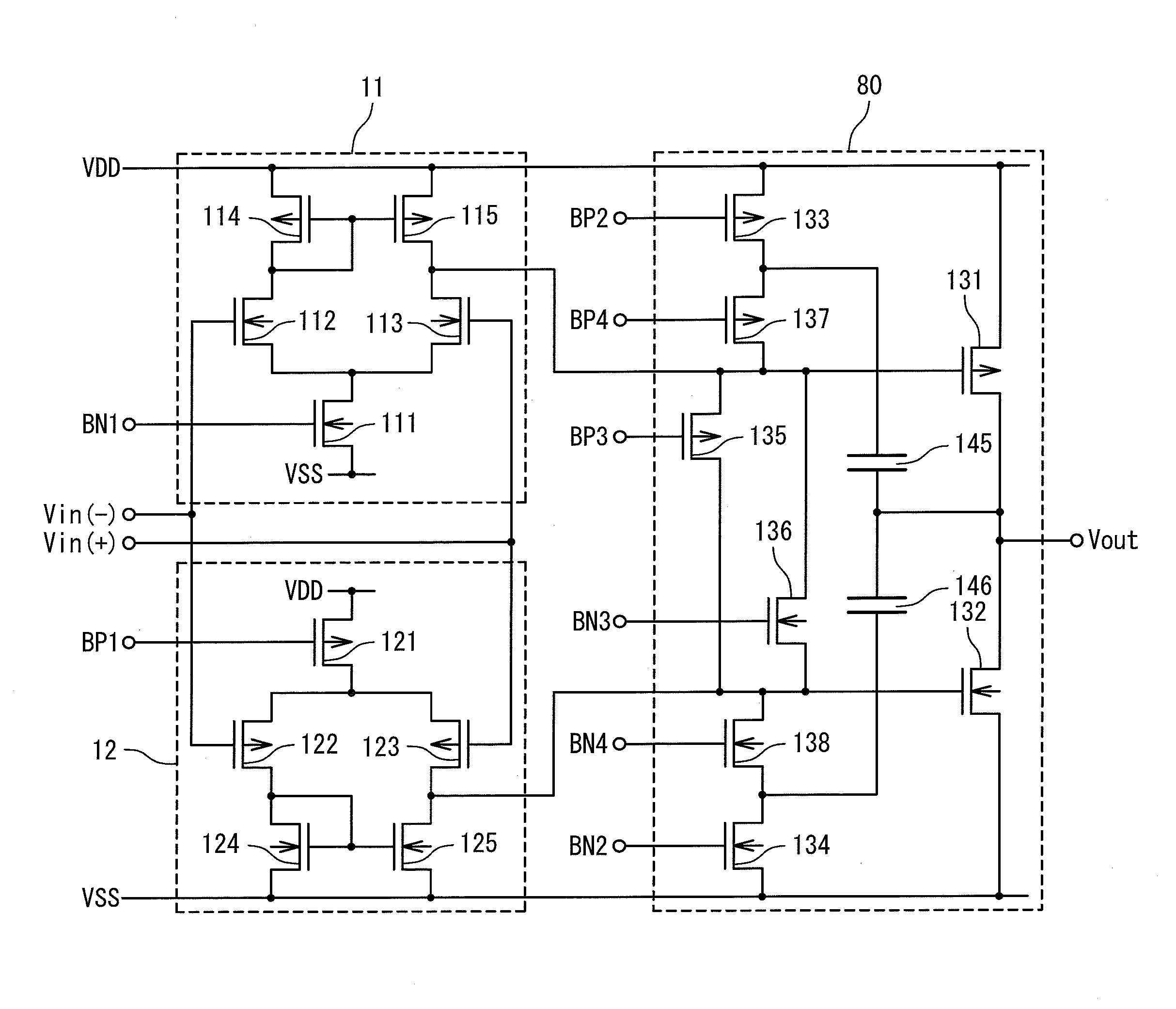
[0033]Hereinafter, a driver circuit, a method of driving a circuit and display device according to an embodiment of the present invention will be described by referring to the accompanying drawings.

[0034]FIG. 4 is a block diagram illustrating a configuration of a display device according to the embodiment of the present invention. The display device includes a driver circuit having a control circuit 4, a gray level power source 5, a scan line driver circuit 6 and a data line driver circuit 7, and a display panel 8. The driver circuit of the display device drives the display panel 8.

[0035]An example of the display panel 8 is an active matrix drive-type color liquid crystal panel using thin film MOS transistors (TFT) as switching elements. Pixels are disposed in a matrix at intersection points of scan lines and data lines which are arranged at predetermined intervals in a row direction and a column direction. Each of the pixels includes a liquid crystal capacitance as an equivalently ...


PUM


Abstract

A driver circuit of the present invention comprises a differential class AB amplifier circuit which comprises: a first differential amplifier circuit configured to amplify differential input signals and output a first signal in a first voltage range; a second differential amplifier circuit configured to amplify the differential input signals and output a second signal in a second voltage range; and a class AB output circuit configured to input the first and the second signals as differential signals and amplify the differential signals, wherein the class AB output circuit comprises: a phase compensating capacitance section; and a current buffer circuit configured to control a current flowing thorough the phase compensating capacitance section.

Description

INCORPORATION BY REFERENCE [0001]This application claims the benefit of priority based on Japanese Patent Application No. 2009-162827, filed on Jul. 9, 2009, the disclosure of which is incorporated herein by reference.BACKGROUND OF THE INVENTION[0002]1. Field of the Invention[0003]The present invention relates to a differential class AB amplifier circuit, and a driver circuit and a display device which are provided with the differential class AB amplifier circuit.[0004]2. Description of Related Art[0005]To simultaneously drive a large number of capacitive loads, a display device includes a plurality of differential class AB amplifier circuits as driver circuits. Each of those driver circuits voltage-drives, for example, a data line in each column of an LCD (Liquid Crystal Display) panel and outputs an analog signal corresponding to display data. Thus, it is required to enable so-called Rail-To-Rail input / output in a whole range of a power source voltage, and a voltage follower conne...

Claims


Application Information

Patent Timeline
Patent Type & Authority Applications(United States)
IPC IPC(8): G06F3/038H03F3/45
CPCG09G3/3688H03F3/3022H03F2203/45646H03F3/45219H03F2203/45632H03F3/45183
Inventor HISANO, HARUHIKO
Owner RENESAS ELECTRONICS CORP
Why Eureka
Try Eureka