Semiconductor device and display apparatus

Inactive Publication Date: 2011-01-20
SONY CORP
View PDF11 Cites 16 Cited by
  • Summary
  • Abstract
  • Description
  • Claims
  • Application Information

AI Technical Summary

Benefits of technology

[0010]In the semiconductor device having such a configuration and the display using the semiconductor device, since the exposed surface including the side wall of the organic semiconductor layer is covered with the protective film, the organic semiconductor layer is securely protected by the protective film. Meanwhile, since the protective film is a patterned structure, the area of the interfaces in contact with other layers is reduced, and delamination at the protective film interface can be prevented.
[0011]Furthermore, according to the pr

Problems solved by technology

Therefore, the organic semiconductor layer 105 constituting the channel portion is damaged by the solvent used in the subs

Method used


Image

  • Semiconductor device and display apparatus
  • Semiconductor device and display apparatus
  • Semiconductor device and display apparatus

Examples


first embodiment

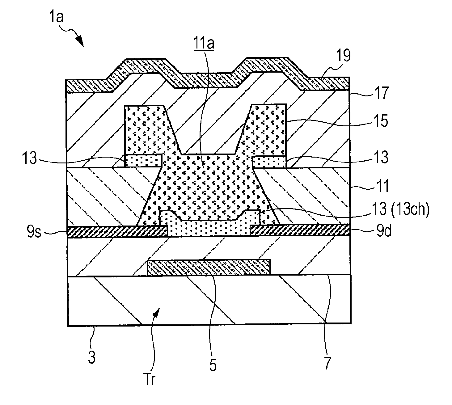
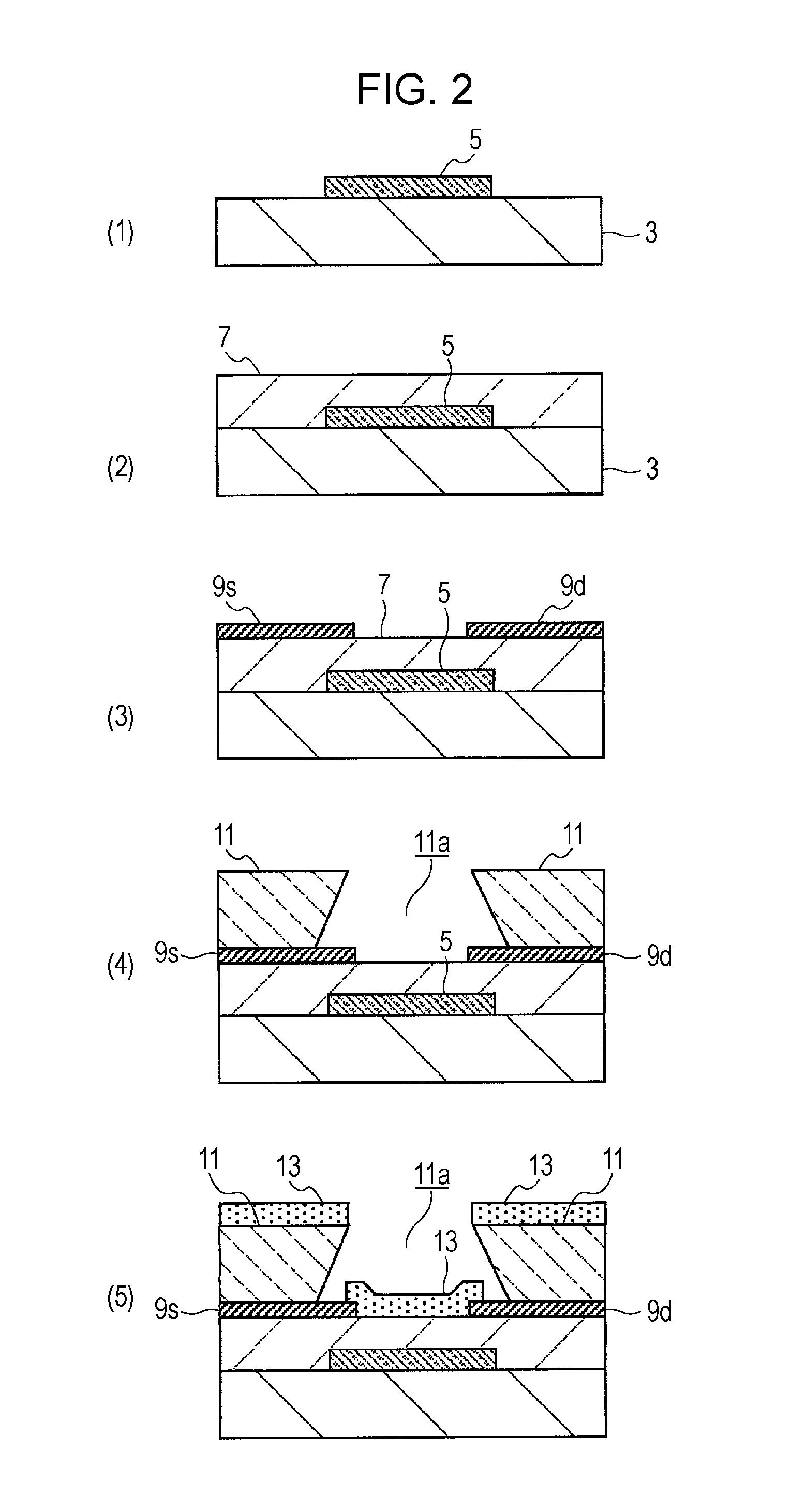
[0028]A semiconductor device 1a shown in FIG. 1 includes a bottom-gate-bottom-contact-type thin film transistor. In the semiconductor device 1a shown in this drawing, a gate electrode 5 composed of a conductive material is formed by patterning on a substrate 3. A gate-insulating film 7 is formed above the substrate 3 in such a state as to cover the gate electrode 5. On the gate-insulating film 7, a pair of a source electrode 9s and a drain electrode 9d composed of a conductive material are formed by patterning at both sides sandwiching the gate electrode 5.

[0029]A partition wall 11 composed of an insulating material is disposed above the substrate 3 provided with the source electrode 9s and the drain electrode 9d. An opening 11a is provided in the partition wall 11, the opening 11a exposing therethrough the surface of the gate-insulating film 7 between the source electrode 9S and the drain electrode 9d and ends of the source electrode 9S and the drain electrode 9d located on the sid...

second embodiment

[0064]A semiconductor device 1b according to a second embodiment shown in FIG. 5 includes a top-gate-bottom-contact-type thin film transistor Tr′. The semiconductor device 1b shown in this drawing differs from the semiconductor device 1a according to the first embodiment described with reference to FIG. 1 in that the gate electrode 5 is disposed on the top of the insulating film 16 which covers the protective film 15, and the other configuration is the same as that of the first embodiment.

[0065]That is, the insulating film 16 is disposed in such a state as to cover the protective film 15, and the protective film 15 and the insulating film 16 constitute a gate-insulating film 7′. The gate electrode 5 composed of a conductive pattern is disposed on the gate-insulating film 7′.

[0066]Consequently, the second embodiment is the same as the first embodiment in that a pair of the source electrode 9s and the drain electrode 9d are formed by patterning on the top of the substrate 3, the parti...

third embodiment

[0086]A semiconductor device 1c according to a third embodiment shown in FIG. 8 includes a bottom-gate-bottom-contact-type thin film transistor Tr. The semiconductor device 1c shown in this drawing differs from the semiconductor device 1a according to the first embodiment described with reference to FIG. 1 in that the partition wall 11 is not disposed, and the other configuration is the same as that of the first embodiment.

[0087]That is, the semiconductor device 1c shown in FIG. 1 includes a bottom-gate-bottom-contact-type thin film transistor tr. In the semiconductor device 1c shown in this drawing, a gate electrode 5 composed of a conductive material is formed by patterning on a substrate 3. A gate-insulating film 7 is formed on the substrate 3 in such a state as to cover the gate electrode 5. On the gate-insulating film 7, a pair of a source electrode 9s and a drain electrode 9d composed of a conductive material are formed by patterning at both sides sandwiching the gate electrod...


PUM


Abstract

A semiconductor device is provided in which, while an organic semiconductor layer is sufficiently protected by a protective film, it is possible to prevent delamination at the protective film interface, thereby achieving good characteristics and improving yield due to improvement in mechanical reliability. A semiconductor device (1a) includes an organic semiconductor layer (13) formed by patterning on a substrate (3), and a protective film (15) formed by patterning on the substrate (3) in such a state as to cover an exposed surface including a side wall of the organic semiconductor layer (13). An insulating partition wall (11) having an opening (11a) is disposed on the substrate (3), and the organic semiconductor layer (13) is formed by patterning, in a state of being divided by the partition wall (11), on the bottom of the opening (11a) of the partition wall (11). Furthermore, the protective film (15) is disposed in such a state as to fill the inside of the opening (11a) of the partition wall (11).

Description

TECHNICAL FIELD[0001]The present invention relates to a semiconductor device and a display, and more particularly, relates to a semiconductor device using an organic semiconductor layer and a display using the semiconductor device.BACKGROUND ART[0002]Thin film transistors are widely used in electronic circuits, in particular, as pixel transistors in active-matrix-driven flat displays. In recent years, use of organic materials for such low-profile semiconductor devices has been receiving attention. In thin film transistors using organic materials for semiconductor layers, i.e., organic thin film transistors (OTFTs), it is possible to form semiconductor layers at a reduced temperature compared to structures in which inorganic materials are used for semiconductor layers. Therefore, organic thin film transistors are advantageous in terms of the increase in area thereof, and can be formed on non-heat-resistant, flexible substrates, such as plastic substrates. An increase in the range of ...

Claims


Application Information

Patent Timeline
IPC IPC(8): H01L51/05
CPCH01L51/0545H01L51/107H01L51/10H10K10/80H10K10/466H10K10/88H10K10/464
Inventor YONEYA, NOBUHIDE
Owner SONY CORP
Why Eureka
Try Eureka