

Electronic control unit
- Summary
- Abstract
- Description
- Claims
- Application Information
AI Technical Summary
Benefits of technology
Problems solved by technology
Method used
Image

Examples
ninth embodiment
[0094]As shown in FIG. 13, in an electronic control unit 9 of the present embodiment, a second low thermal-conductive layer 411 is formed in the circuit board 40 between the circuit pattern 812, on which the A_MOS 31 is placed, and the circuit pattern 832, on which the B_MOS 33 is placed. A second low thermal-conductive layer 421 is formed in the circuit board 40 between the circuit pattern 822, on which the A′_MOS 32 is placed, and the circuit pattern 842, on which the B′_MOS 34 is placed.
[0095]The second low thermal-conductive layers 411, 421 are made of the same material with the first low thermal-conductive layers 912, 922, 932, 942 described in the fourth embodiment, and extend along an extending direction of the circuit board 40.
[0096]In the present embodiment, the thermal interference between the A_MOS 31 and the B_MOS 33 can be limited by reducing the thermal conduction between the circuit patterns 812, 832 which are formed respectively on the surface of the circuit board 40...
tenth embodiment
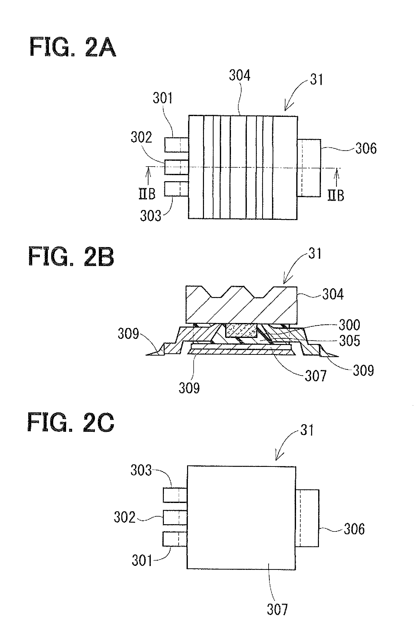
[0097]As shown in FIG. 14, in an electronic control unit 10 of the present embodiment, the B_MOS 33 and the B′_MOS 34, which are placed on the rear surface of the circuit board 40, are placed away from each of locations directly below the A_MOS 31 and the A′_MOS 32, which are placed on the surface of the circuit board 40.
[0098]The through hole 400 and the inner layer patterns as a thermal conducting path means are formed directly below each of the MOSs 31 to 34. A ninth to eleventh thermal-conduction limiting portions 43, 44, 45 are formed between adjacent through holes 400 which are formed directly below the MOSs 31 to 34. As with the seventh and eighth thermal-conduction limiting portions 41, 42 described in the sixth embodiment, the ninth to eleventh thermal-conduction limiting portions 43, 44, 45 are made of resin configuring the circuit board. The inner layer patterns are not formed in the ninth to eleventh thermal-conduction limiting portions 43, 44, 45. Since the thermal resi...
eleventh embodiment
[0100]As shown in FIG. 15, in an electronic control unit 11 of the eleventh embodiment, second low thermal-conductive layers 431, 441, 451 are formed between the adjacent through holes 400 and the inner layer patterns, which are formed directly below the MOSs 31 to 34. The second low thermal-conductive layers 431, 441, 451 are made of the same material with the first low thermal-conductive layers 912, 922, 932, 942 and the second low thermal-conductive layers 411, 421 described in the fourth and ninth embodiments.
[0101]In the present embodiment, the thermal interference between the MOSs 31 to 34 can be limited reliably by reducing the thermal conduction between the circuit patterns 812, 822, 832, 842, which are formed on the surface and the rear surface of the circuit board 40. Furthermore, heat generated from the MOSs 31 to 34 can be released to the opposite side of the circuit board 40 easily by forming the thermal conducting path means directly below the MOSs 31 to 34.
PUM
 Abstract
Description
Claims
Application Information