

Emi/rf shielding of thermocouples
a technology of rf shielding and thermocouple, which is applied in the field of thermocouple shielding, can solve the problems that the rf power may have a negative impact achieve the effects of reducing the negative impact of the rf power on the temperature sensor, accurate temperature measurement, and reducing the negative impa
- Summary
- Abstract
- Description
- Claims
- Application Information
AI Technical Summary
Benefits of technology
Problems solved by technology
Method used
Image

Examples
Embodiment Construction
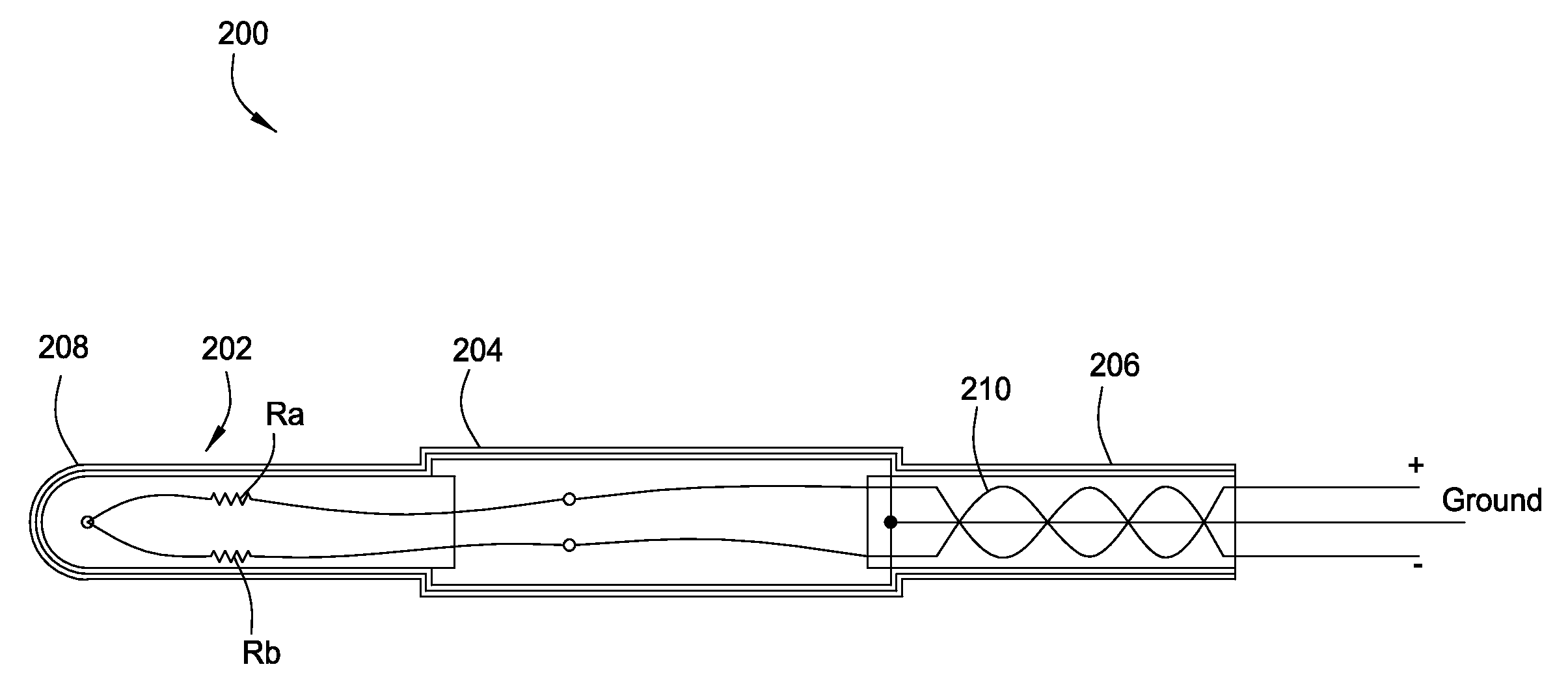
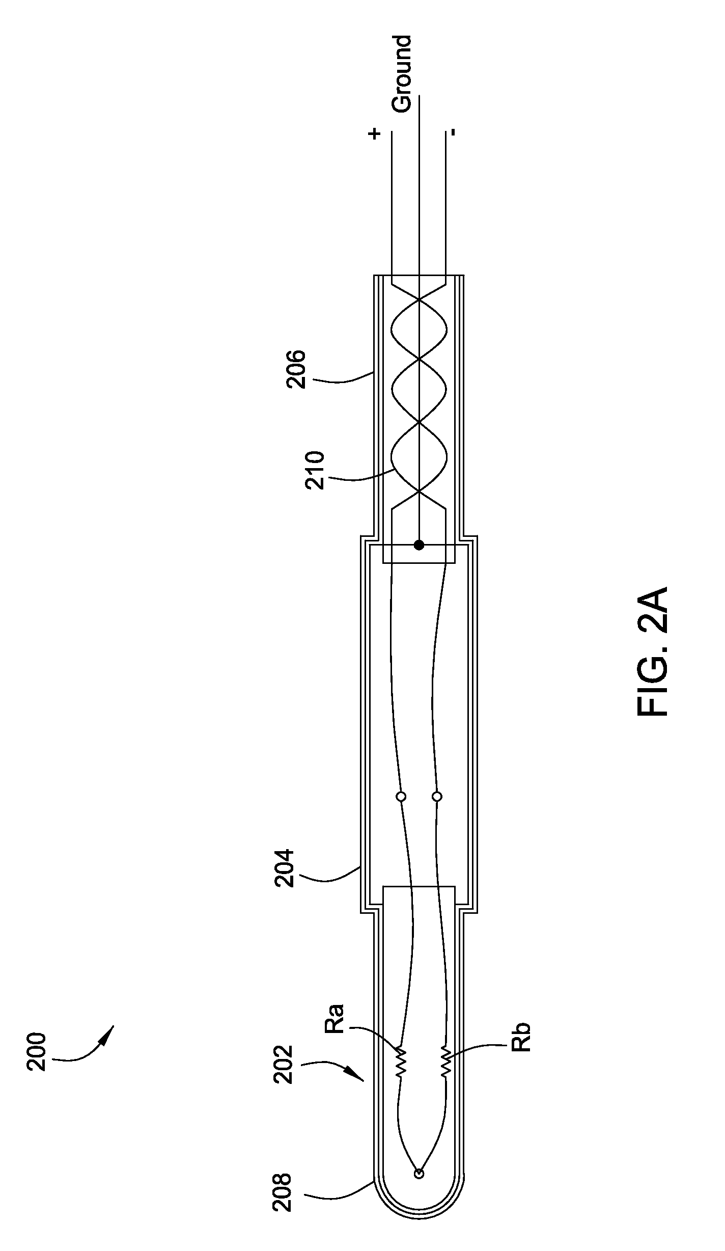
[0020]Embodiments disclosed herein generally relate to a temperature sensor disposed in an apparatus. In many semiconductor, liquid crystal display, solar panel or organic light emitting display fabrication processes, RF power is utilized to either ignite a plasma within the processing chamber or to provide supplemental energy to the process. Temperature control during many processes may be beneficial in order to produce a consistent product. Temperature sensors or thermocouples are sometimes utilized to measure the temperature of a substrate within a processing chamber. The RF power may have a negative impact on the temperature sensor. By coating the temperature sensor with a nanoparticle based metal coating, such as a silver coating, the negative impacts of the RF power on the temperature sensor may be reduced without contaminating the process, and an accurate temperature measurement may be obtained.
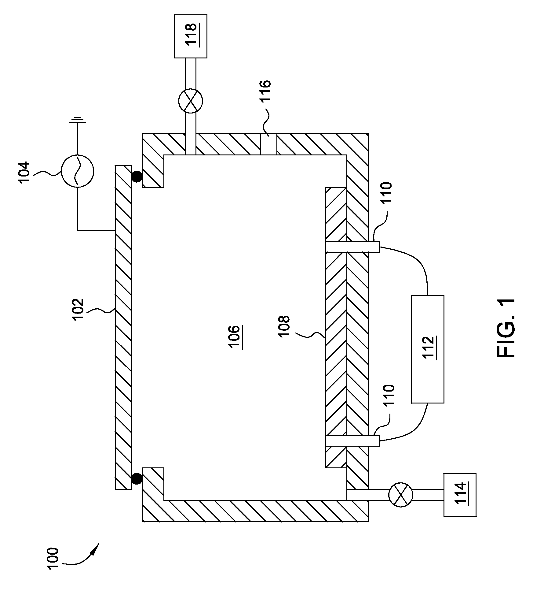
[0021]FIG. 1 is a schematic cross-sectional view of an apparatus having a pluralit...
PUM
 Abstract
Description
Claims
Application Information