Heat treatment apparatus, computer program, and storage medium

a heat treatment apparatus and computer program technology, applied in lighting and heating apparatus, household stoves or ranges, furnaces, etc., can solve the problems of not being able to quickly lower the temperature and not being able to cope with the new design rule, so as to achieve excellent operational effects, improve heating efficiency, and improve heating efficiency.

Active Publication Date: 2008-08-07
TOKYO ELECTRON LTD
View PDF14 Cites 22 Cited by
  • Summary
  • Abstract
  • Description
  • Claims
  • Application Information

AI Technical Summary

Benefits of technology

[0044]The heat treatment apparatus and the storage medium in accordance with the present invention provide following excellent operational effects.
[0045]By forming the plurality of thermoelectric conversion elements at the mounting table and disposing the semiconductor light emitting elements above it, in case of heating the target object, a current flows to the thermoelectric conversion elements in such a direction so as to heat the target object and the semiconductor light emitting elements are turned on, whereby light for heating is emitted to heat the target object. On the contrary, in case of cooling the target object, the current flows to the thermoelectric conversion elements in such a direction so as to cool the target object and the semiconductor light emitting elements are turned off. Therefore, heating efficiency is more improved than lamp heating and it is possible to realize higher-speed temperature elevation and reduction.
[0046]In accordance with the present invention, since the reflected light by each first reflector is focused on an individual area of the target object, the distribution of illumination intensity on the surface of the target object can be uniform, thereby making it possible to improve the in-surface temperature uniformity.
[0047]Further, in accordance with the present invention, since the measurement wavelength band of the radiation thermometer is set different from that of the light emitted from the semiconductor light emitting elements, stray light for the radiation thermometer is removed, thus making it possible to accurately measure the temperature by using the radiation thermometer.

Problems solved by technology

However, as a design rule of a line width, a film thickness or the like becomes strict, the temperature of the wafer is required to be controlled at a high speed, but it is not possible to rapidly lower the temperature by using the above-mentioned conventional apparatus, which cannot cope with the new design rule.

Method used


Image

  • Heat treatment apparatus, computer program, and storage medium
  • Heat treatment apparatus, computer program, and storage medium
  • Heat treatment apparatus, computer program, and storage medium

Examples


first preferred embodiment

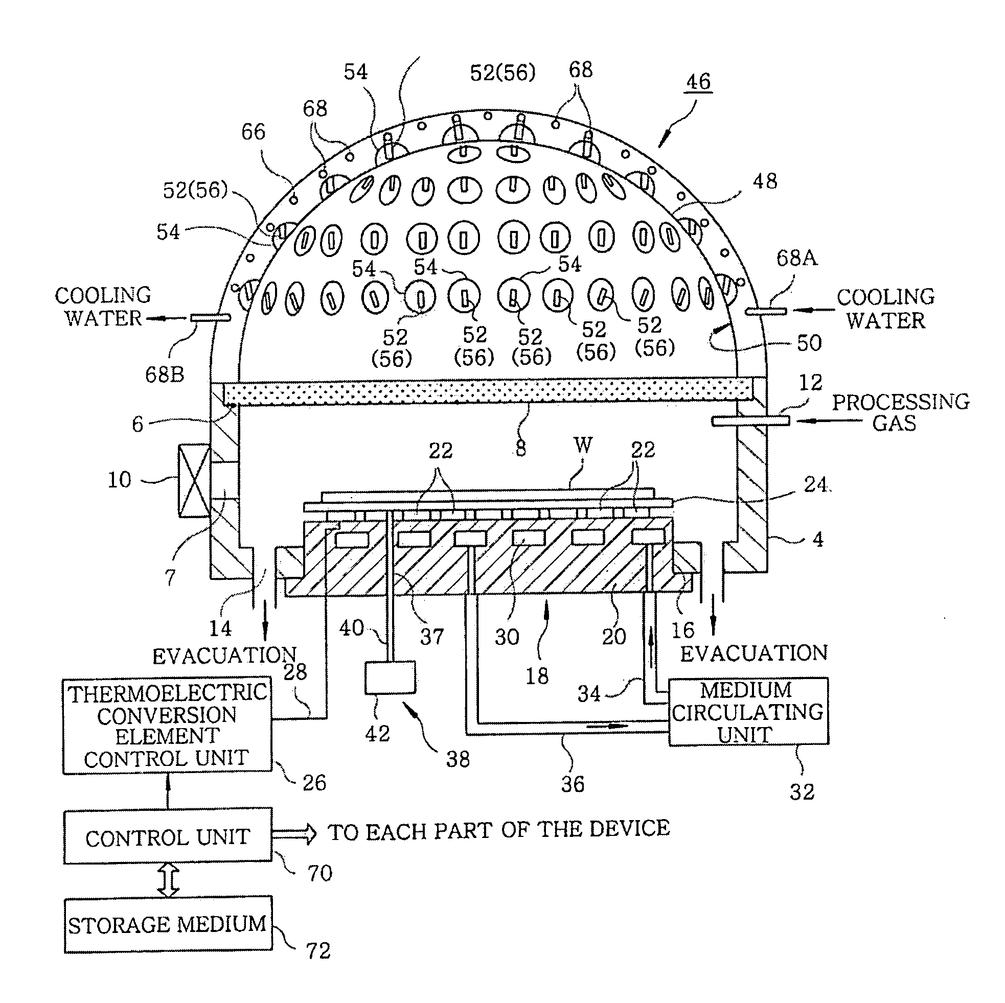
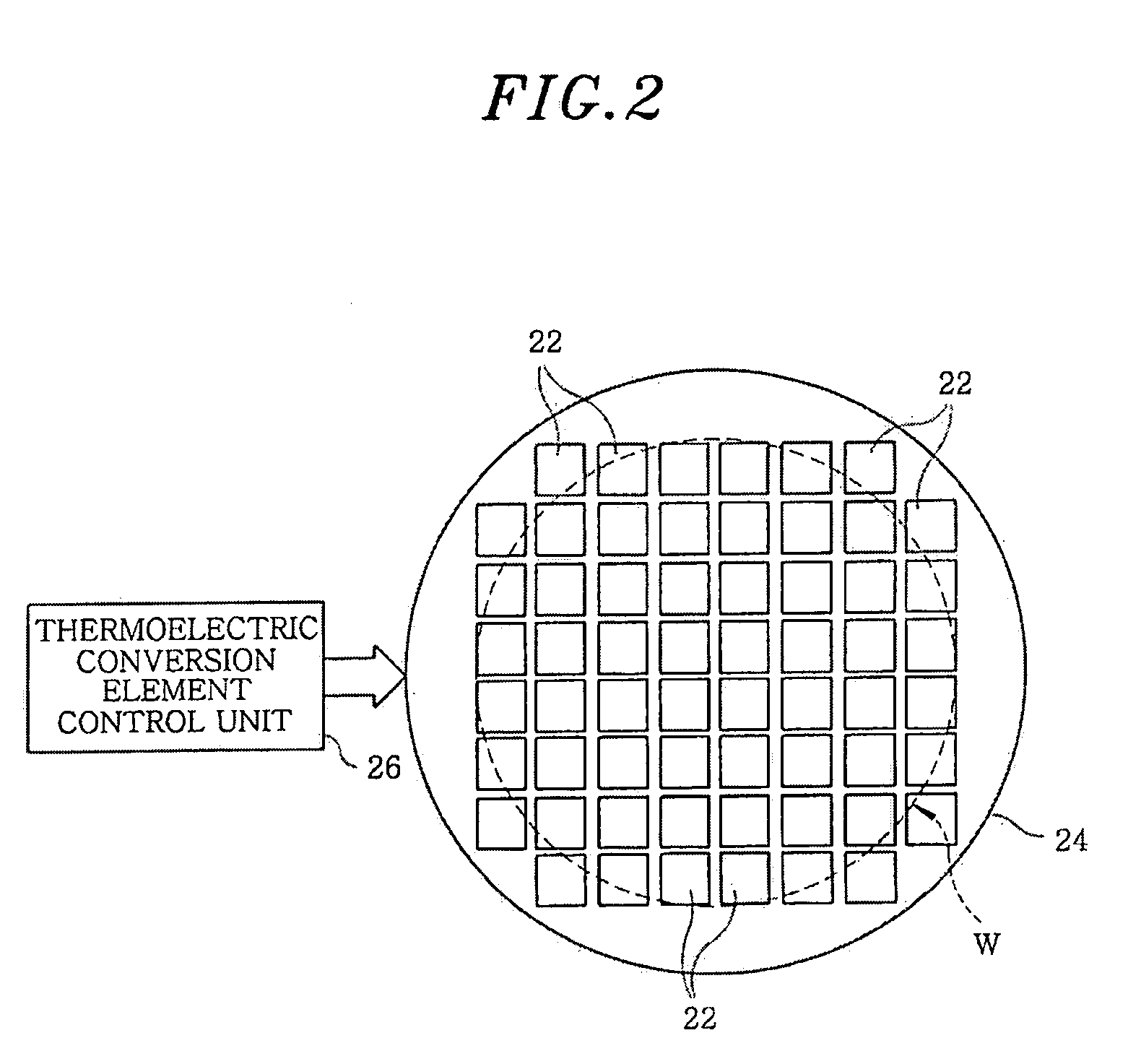
[0060]FIG. 1 provides a cross sectional configuration view of a heat treatment apparatus of the first preferred embodiment of the present invention, FIG. 2 shows a plan view of an arrangement of a thermoelectric conversion element, FIG. 3 illustrates a path of light to be used for heating generated from a semiconductor light emitting element of a light source, FIG. 4 is an enlarged cross-sectional view representing an element attachment rod where the semiconductor light emitting element is attached, and FIG. 5 is an enlarged perspective view describing an end portion of the element attachment rod.

[0061]As shown in FIG. 1, a heat treatment apparatus 2 of the first preferred embodiment includes, for example, a processing chamber 4 of a housing shape made of aluminum. The processing chamber 4 is configured to accommodate a semiconductor wafer having a diameter of, e.g., 300 mm. A ceiling portion of the processing chamber 4 is opened, while airtightly installed in this opening through a...

second preferred embodiment

[0095]Hereinafter, the second preferred embodiment of the heat treatment apparatus in accordance with the present invention will be described. While the above-described first preferred embodiment has been described with respect to the case of the element attachment housing 48 of a dome shape like a substantially hemispheric shape, the second preferred embodiment will be described in detail with respect to the case of a substantially flat element attachment housing 48.

[0096]FIG. 6 provides a cross sectional view showing the heat treatment apparatus in accordance with the second preferred embodiment of the present invention, FIG. 7 shows a plan view showing an arrangement of a specified number of semiconductor light emitting elements block-partitioned into a plurality of modules on an element installation substrate, FIG. 8 illustrates an enlarged cross sectional view showing an arrangement of the element installation substrate, FIG. 9 is an enlarged plan view describing an example of ...

third preferred embodiment

[0114]Hereinafter, the third preferred embodiment of the heat treatment apparatus in accordance with the present invention will be described. Although the above-described first and second preferred embodiments have been described with respect to the case of the mounting table 18 provided with the thermoelectric conversion element 22 formed of the peltier element, the present invention is not limited thereto, and may use a common mounting table conventionally used.

[0115]FIG. 11 provides a cross sectional view showing the heat treatment apparatus in accordance with the third preferred embodiment of the present invention.

[0116]Herein, a heating unit 46 with the element attachment housing 82 of a planar shape of the second preferred embodiment shown in FIG. 6 disposed at the ceiling portion of a processing chamber is exemplified. Further, identical reference numerals will be used for the same parts described in FIGS. 1 to 10 and description thereof will be omitted.

[0117]As shown in FIG....


PUM


Abstract

A heat treatment apparatus for performing prescribed heat treatment to a subject (W) to be treated is provided with a processing chamber in which air can be exhausted; a mounting table arranged in the processing chamber, for placing on an upper plane the subject to be treated; a plurality of thermoelectric conversion elements arranged on an upper part of the mounting table; a light transmitting window for covering a ceiling portion of the processing chamber airtight; and a gas introduction unit for introducing a required gas into the processing chamber. A heating unit which includes a plurality of heating light sources including a semiconductor light emitting element for emitting heating light to the subject to be treated, is provided above the light transmitting window. Thus, heating efficiency is improved and temperature can be increased and reduced at a higher speed for the subject to be treated.

Description

[0001]This application is a Continuation Application of PCT International Application No. PCT / JP2006 / 318031 filed on Sep. 12, 2006, which designated the United States.FIELD OF THE INVENTION[0002]The present invention relates to a single-wafer heat treatment apparatus, a computer program and a storage medium for performing a specified heat treatment on a semiconductor wafer or the like by irradiating light for heating thereto.BACKGROUND OF THE INVENTION[0003]Generally, in order to fabricate a desired semiconductor device, various heat treatment processes such as a film forming process, a pattern etching process, an oxidation / diffusion process, a quality modification process, an annealing process and the like are repeatedly performed on a semiconductor device. With a recent trend towards a high-density, a multilayered structure and high-integration of the semiconductor device, means employed therefor has been getting more tightly restricted, and especially, an improvement of in-surfac...

Claims


Application Information

Patent Timeline
Patent Type & Authority Applications(United States)
IPC IPC(8): F26B3/30
CPCH01L21/324H01L21/67115H01L21/67109
Inventor SHIMIZU, MASAHIROKASAI, SHIGERUYONEDA, MASATAKE
Owner TOKYO ELECTRON LTD
Why Eureka
Try Eureka