Chip on glass type LCD device and inspecting method of the same

a technology of liquid crystal display and inspection method, which is applied in the direction of measurement devices, electrical testing, instruments, etc., can solve the problems of block dim effect, difference between thin film transistors, and non-uniform etching

Active Publication Date: 2011-01-27
LG DISPLAY CO LTD
View PDF3 Cites 56 Cited by
  • Summary
  • Abstract
  • Description
  • Claims
  • Application Information

AI Technical Summary

Benefits of technology

[0033]An advantage of the present invention is to provide a COG type LCD device and an inspecting method of the same that include testing lines and testing pads to detect block dim effects before attaching a driving IC.
[0034]Additional features and advantages of the invention will be set forth in the description which follows, and in part will be apparent from the description, or may be learned by practice of the invention. The objectives and other advantages of the invention will be realized and attained by the structure particularly pointed out in the written description and claims hereof as well as the appended drawings.
[0035]To achieve these and other advantages and in accordance with the purpose of the present invention, as embodied and broadly described herein, a COG type LCD device includes a first substrate including a display area and a non-display area surrounding the display area, wherein the non-display area includes first, second, third and fourth non-display areas, gate and data lines in the display area on the first substrate and crossing each other to define pixel regions, switching thin film transistor at each crossing portion of the gate and data lines and connected to the gate and data lines, a pixel electrode in each pixel region and connected to the thin film transistor, first testing thin film transistors in the second non-display area and connected to the data lines, the first testing thin film transistors spaced apart from each other with a constant interval therebetween, first, second and third data testing lines connected to one ends of the data lines through the first testing thin film transistors, wherein the first data testing line is connected to (3n-2)th data lines, the second data testing line is connected to (3n-1)th data lines, and the third data testing line is connected to (3n)th data lines, wherein n is a natural number, first, second and third data testing pads connected to the first, second and third data testing lines, respectively, data link lines in the first non-display area and connected to another ends of the data lines, second testing thin film transistors in the first non-display area and connected to the data link lines, gate link lines connected to the gate lines, third testing thin film transistors connected to the gate link lines, gate testing lines connected to the gate lines through the third testing thin film transistors, gate testing pads connected to the gate testing lines, a common testing line and a

Problems solved by technology

Accordingly, the first, second and third testing thin film transistors have different characteristics, and this causes block dim effects during the lighting inspection of the COG type LCD device.
There is the difference between the thin film transistors due to the no

Method used


Image

  • Chip on glass type LCD device and inspecting method of the same
  • Chip on glass type LCD device and inspecting method of the same
  • Chip on glass type LCD device and inspecting method of the same

Examples


Embodiment Construction

[0044]Reference will now be made in detail to the preferred embodiment, an example of which is illustrated in the accompanying drawings.

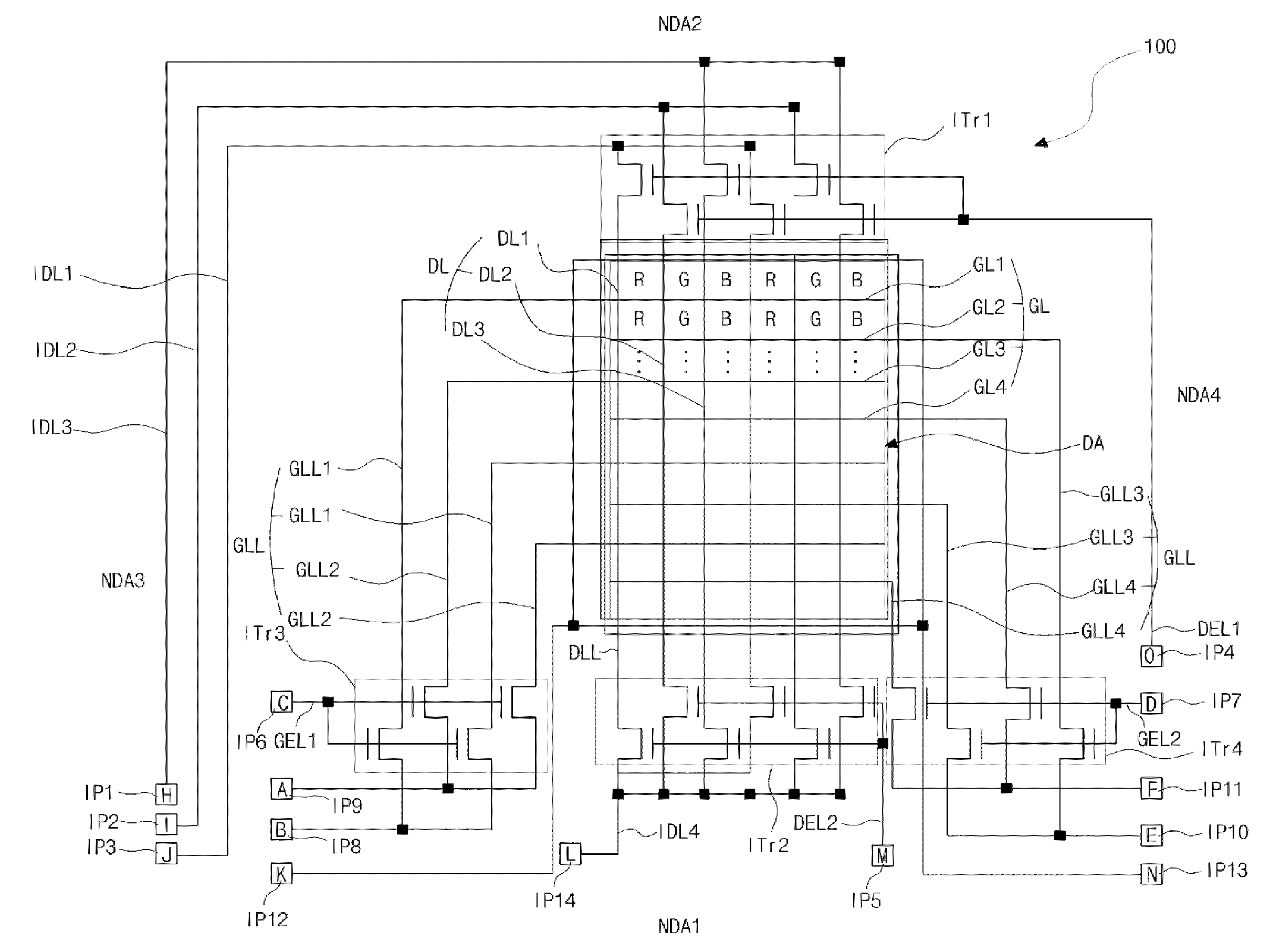
[0045]FIG. 4 is a view of schematically illustrating a COG type LCD device according to an embodiment of the present invention. For convenience of explanation, FIG. 4 mainly shows a structure of an array substrate.

[0046]In FIG. 4, the COG type LCD device 100 includes a display area DA and first, second, third and fourth non-display areas NDA1, NDA2, NDA3 and NDA4 outside the display area DA. The first, second, third and fourth non-display areas NDA1, NDA2, NDA3 and NDA4 surround the display area DA. The first, second, third and fourth non-display areas NDA1, NDA2, NDA3 and NDA4 may be disposed at lower, upper, left and right sides of the display area DA, respectively, in the context of the figure.

[0047]Gate lines GL and data lines DL are formed in the display area DA on an array substrate and cross each other to define pixel regions P. A switching t...


PUM


Abstract

A COG type LCD device includes a first substrate including a display area and first, second, third and fourth non-display areas, gate and data lines in the display area on the first substrate and defining pixel regions, switching thin film transistor at each crossing portion of the gate and data lines and connected to the gate and data lines, a pixel electrode in each pixel region and connected to the thin film transistor, first testing thin film transistors in the second non-display area connected to the data lines and spaced apart from each other with a constant interval therebetween, first, second and third data testing lines connected to one ends of the data lines through the first testing thin film transistors, first, second and third data testing pads connected to the first, second and third data testing lines, respectively, data link lines in the first non-display area and connected to another ends of the data lines, second testing thin film transistors in the first non-display area and connected to the data link lines, gate link lines connected to the gate lines, third testing thin film transistors connected to the gate link lines, gate testing lines connected to the gate lines through the third testing thin film transistors, gate testing pads connected to the gate testing lines, a common testing line and a common pad in the non-display area, a second substrate spaced apart from the first substrate, a color filter layer and a common electrode sequentially formed on the second substrate, wherein the common electrode is connected to the common testing line, and a liquid crystal layer between the first and second substrates, wherein a driving IC is attached in the first non-display area.

Description

[0001]The present application claims the benefit of Korean Patent Application No. 10-2009-0066213 filed in Korea on Jul. 21, 2009, which is hereby incorporated by reference.BACKGROUND OF THE INVENTION[0002]1. Field of the Invention[0003]The present invention relates to a liquid crystal display (LCD) device, and more particularly to a chip on glass (COG) type LCD device and an inspecting method of the same.[0004]2. Discussion of the Related Art[0005]With the rapid development in information technology, flat panel display (FPD) devices having thin thickness, light weight, and lower power consumption have been introduced and developed.[0006]Among these devices, liquid crystal display (LCD) devices are most widely used for monitors of notebook computers, monitors of personal computers and televisions due to high definition, high qualities, excellent moving images and high contrast ratio.[0007]An LCD device includes two substrates and a liquid crystal layer interposed between the two sub...

Claims


Application Information

Patent Timeline
IPC IPC(8): G02F1/136G01R31/02G01R31/26
CPCG02F1/1345G02F1/13454G09G3/3648G09G3/006G02F1/136286G02F1/13
Inventor KIM, BUNG-GOOKIM, KA-KYUNG
Owner LG DISPLAY CO LTD
Why Eureka
Try Eureka