Ball grid array printed circuit board, package structure, and fabricating method thereof

Inactive Publication Date: 2011-02-03
QUANTA COMPUTER INC +1
View PDF6 Cites 3 Cited by
  • Summary
  • Abstract
  • Description
  • Claims
  • Application Information

AI Technical Summary

Problems solved by technology

Therefore, the dielectric material crack under the pad would be easily occurred.

Method used


Image

  • Ball grid array printed circuit board, package structure, and fabricating method thereof
  • Ball grid array printed circuit board, package structure, and fabricating method thereof
  • Ball grid array printed circuit board, package structure, and fabricating method thereof

Examples


Embodiment Construction

[0016]Reference will now be made in detail to the present embodiments of the invention, examples of which are illustrated in the accompanying drawings. Wherever possible, the same reference numbers are used in the drawings and the description to refer to the same or like parts.

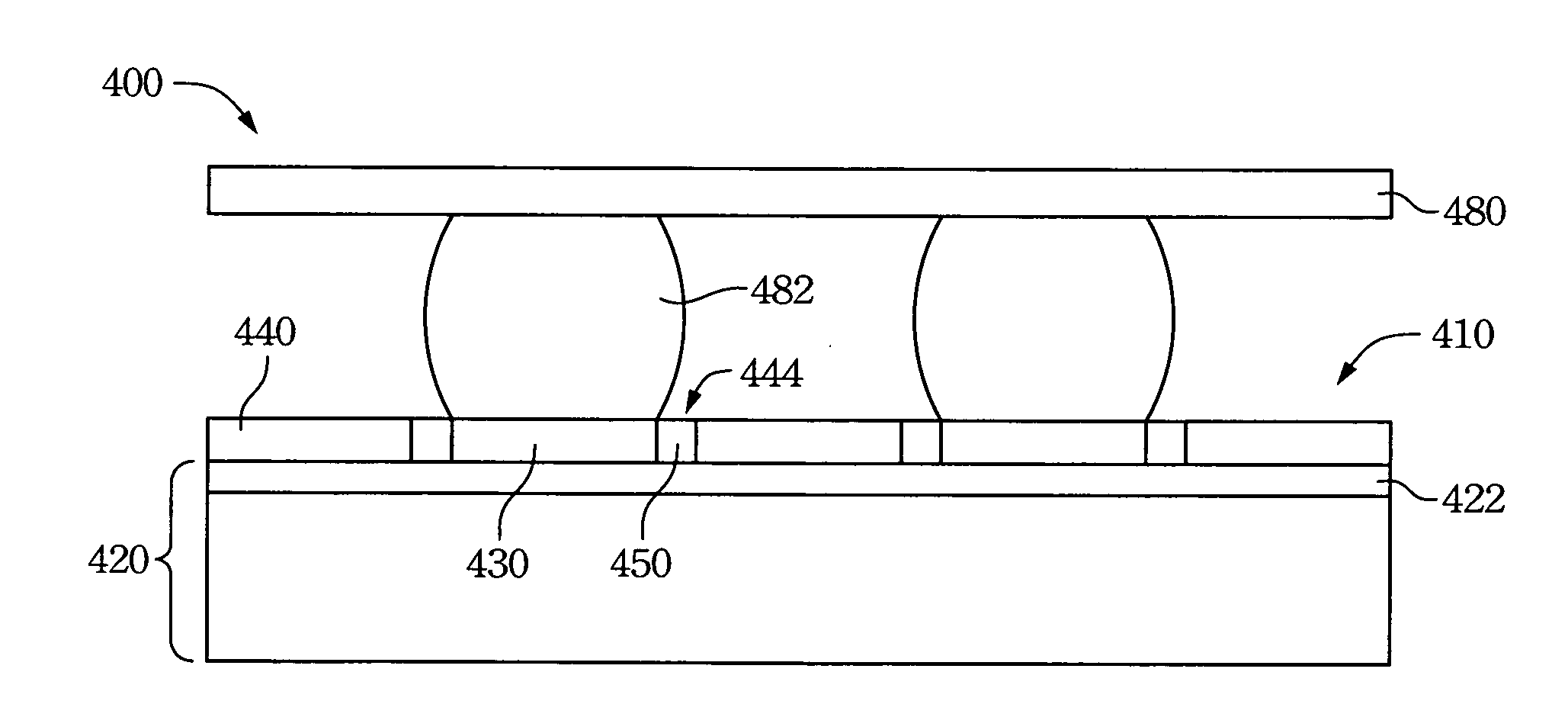
[0017]The dielectric material layer under the grid ball array (BGA) pad may be easily cracked in the conventional lead free BGA printed circuit board process. The applicant found that those cracks of the dielectric material layers have a similar trend, which is started at the gap between the BGA pad and the solder mask, so that the applicant believed that the bonding strength between the dielectric material layer and the BGA pad at the gap is weaker than other (or have to be enhanced).

[0018]The present embodiments provide a ball grid array printed circuit board to enhance the bonding strength between the dielectric material layer and the BGA pad at the gap.

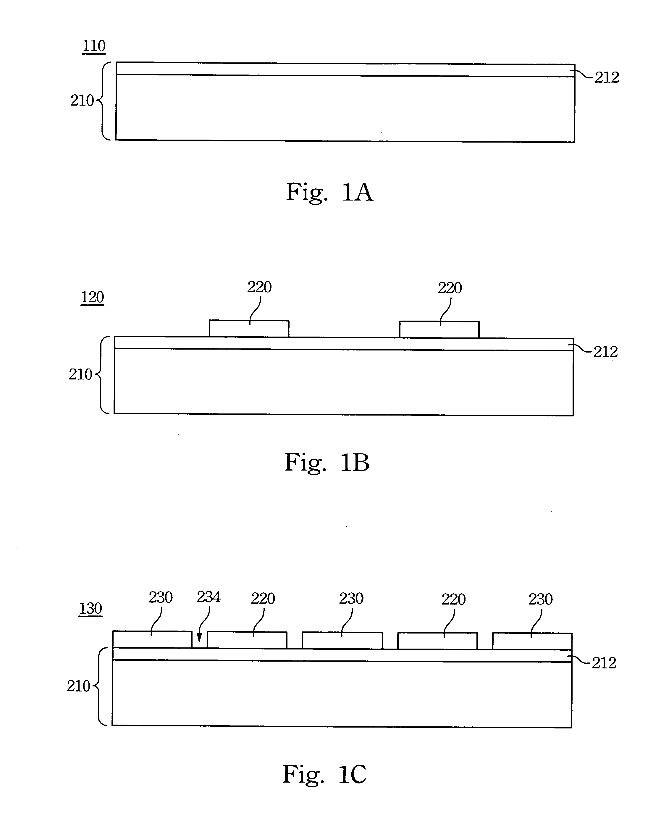
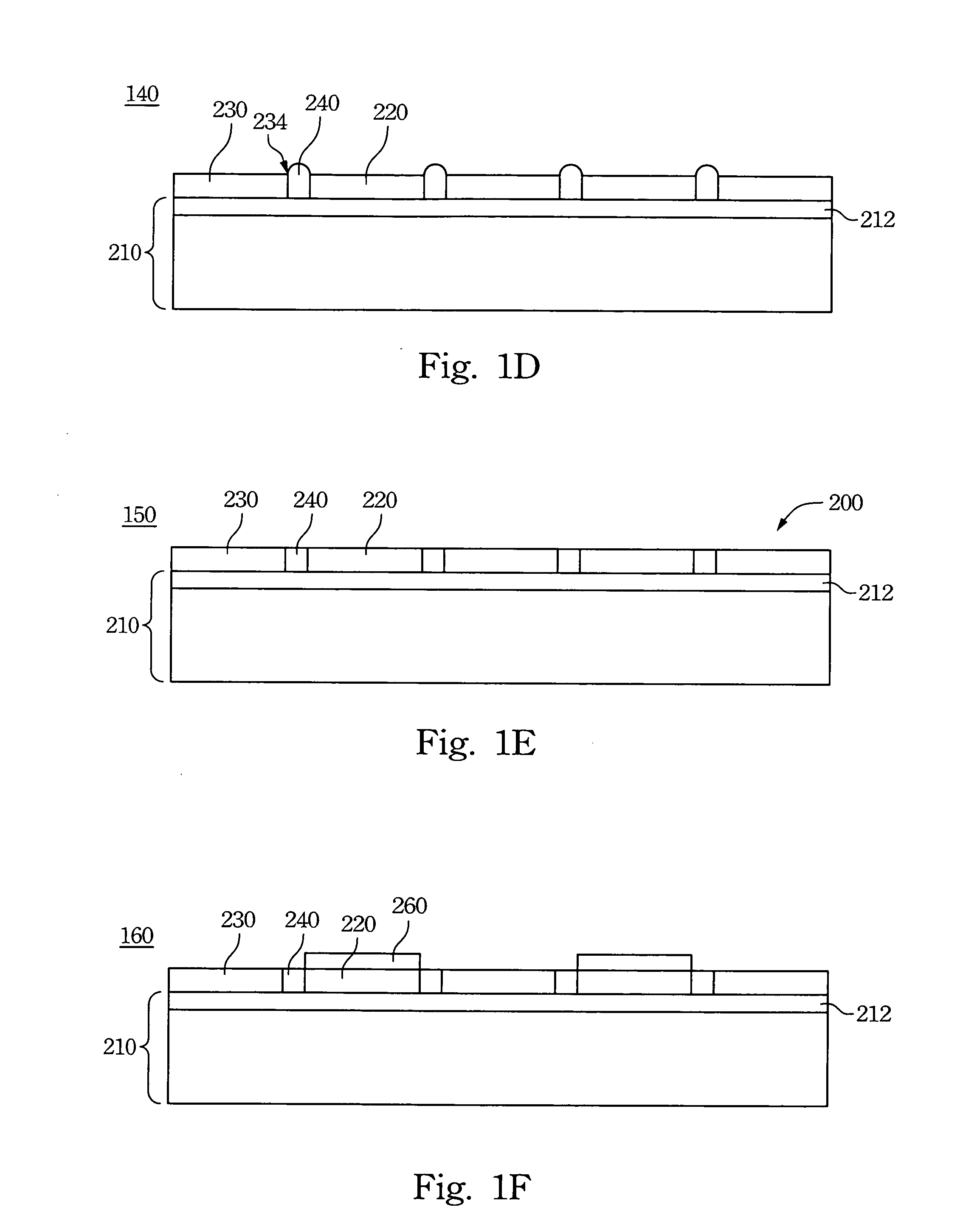
[0019]Refer to FIG. 1A to FIG. 1H. FIG. 1A to FIG. 1H ...


PUM


Abstract

A BGA (ball grid array) printed circuit board is disclosed, which includes a substrate having a dielectric layer, a BGA pad and a solder mask formed on the dielectric layer, and an adhesive glue filled in a gap between the BGA pad and the solder mask. A BGA printed circuit board package structure and a method for fabricating the BGA printed circuit board are also disclosed.

Description

RELATED APPLICATIONS[0001]This application claims priority to Taiwan Application Serial Number 98125399, filed Jul. 28, 2009, which is herein incorporated by reference.BACKGROUND[0002]1. Field of Invention[0003]The present invention relates to a ball grid array printed circuit board. More particularly, the present invention relates to a non-solder mask defined ball grid array printed circuit board.[0004]2. Description of Related Art[0005]Access to an electrical connection with an external circuit is required for an IC chip to function properly, and an IC device has to be packaged to prevent damage from external force or environmental factors during conveyance or pick-and-place procedures. Electronic packaging is a necessary process in integrated circuit production to allow the IC device to perform a predefined function under an organized structure and provides protection.[0006]A ball grid array (BGA) package has been a widely used electronic package structure in integrated circuit p...

Claims


Application Information

Patent Timeline
IPC IPC(8): H05K1/16H05K1/11H05K3/00
CPCH05K3/3436H05K3/3452Y10T29/49149H05K2203/058H05K2203/0597H05K2201/10734
Inventor WU, JIN-CHANGWANG, WEN-BINGWANG, XUN
Owner QUANTA COMPUTER INC
Why Eureka
Try Eureka