Electrophoretic display device and method of fabricating the same

Inactive Publication Date: 2011-02-03
LG DISPLAY CO LTD
View PDF10 Cites 72 Cited by
  • Summary
  • Abstract
  • Description
  • Claims
  • Application Information

AI Technical Summary

Benefits of technology

[0030]Accordingly, the present invention is directed to an electrophoretic display device and method of fabricating th

Problems solved by technology

However, there are disadvantages in the above-mentioned fabricating process for the related art electrophoretic display device.
Accordingly, the fabricating process is very complicated.
Furthermore, when the unessential elements, which are required in the fabricating process for the electrophoretic display device but are not required in the completed electrophoretic display d

Method used


Image

  • Electrophoretic display device and method of fabricating the same
  • Electrophoretic display device and method of fabricating the same
  • Electrophoretic display device and method of fabricating the same

Examples


Embodiment Construction

[0053]Reference will now be made in detail to the illustrated embodiments of the present invention, which are illustrated in the accompanying drawings.

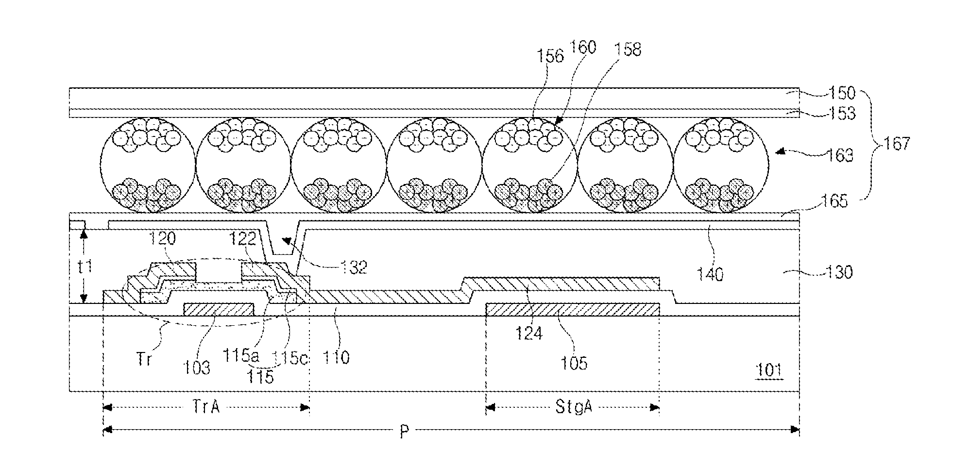
[0054]In an electrophoretic display device according to the present invention, both a film-type ink layer and a color filter layer are formed on an array substrate including thin film transistors.

[0055]FIGS. 4A to 4H, FIGS. 5A to 5H, and FIGS. 6A to 6H are cross-sectional views of illustrating an electrophoretic display device in steps of a fabricating process according to a first embodiment of the present invention. FIGS. 7A to 7C are plan views of illustrating an electrophoretic display device in steps of a fabricating process according to the first embodiment of the present invention. FIGS. 4A to 4H show a pixel region, where a thin film transistor and a storage capacitor are formed, of an electrophoretic display device. FIGS. 5A to 5H show a gate pad region of an electrophoretic display device. FIGS. 6A to 6H show a data pad regio...


PUM


Abstract

An electrophoretic display device includes a switching element on a substrate including a display area having a pixel region and a non-display area at a periphery of the display area, a passivation layer covering the switching element, a pixel electrode on the passivation layer and connected to the switching element, an electrophoresis film on the pixel electrode and including an ink layer and a base film, wherein the ink layer includes a plurality of charged particles, and the base film is formed of polyethylene terephthalate, a common electrode for generating an electric field with the pixel electrode to drive the electrophoresis film, and a color filter layer directly on the electrophoresis film, wherein the color filter layer is formed under temperatures of less than 100 degrees of Celsius.

Description

[0001]The present invention claims the benefit of Korean Patent Application No. 10-2009-0071190, filed in Korea on Aug. 3, 2009, which is hereby incorporated by reference in its entirety.BACKGROUND OF THE INVENTION[0002]1. Field of the Invention[0003]The present invention relates to an electrophoretic display device, and more particularly, to an electrophoretic display device and a method of fabricating the same.[0004]2. Discussion of the Related Art[0005]In general, liquid crystal display (LCD) devices, plasma display panels (PDPs) and organic electro-luminescence displays (OELDs) have been widely used for display devices. However, recently, to meet rapidly diversified consumers' requirements, various display devices has been introduced.[0006]Particularly, properties of a light weight, thin profile, high efficiency and function for displaying full color moving images have been required in the display devices. To satisfy the properties, electrophoretic display devices, which have me...

Claims


Application Information

Patent Timeline
IPC IPC(8): G02F1/167H01J9/24G02F1/16756G02F1/16766G02F1/1677
CPCG02F1/133514G02F2001/1635G02F1/167G02F1/1677G02F1/16756G02F1/16766G02F2203/055G02F2201/50G02F1/133345G02F1/133512G02F1/133516G02F1/136227G02F1/1368
Inventor KWON, OH-NAMCHOI, NACK-BONGPARK, CHOON-HOLIM, YU-SOKLEE, JONG-KWON
Owner LG DISPLAY CO LTD
Why Eureka
Try Eureka