Nitride-based semiconductor device and method for fabricating the same
- Summary
- Abstract
- Description
- Claims
- Application Information
AI Technical Summary
Benefits of technology
Problems solved by technology
Method used
Image

Examples
Embodiment Construction
[0049]Hereinafter, preferred embodiments of the present invention will be described with reference to the accompanying drawings. In the drawings, any elements shown in multiple drawings and having substantially the same function will be identified by the same reference numeral for the sake of simplicity. It should be noted, however, that the present invention is in no way limited to the specific preferred embodiments to be described below.
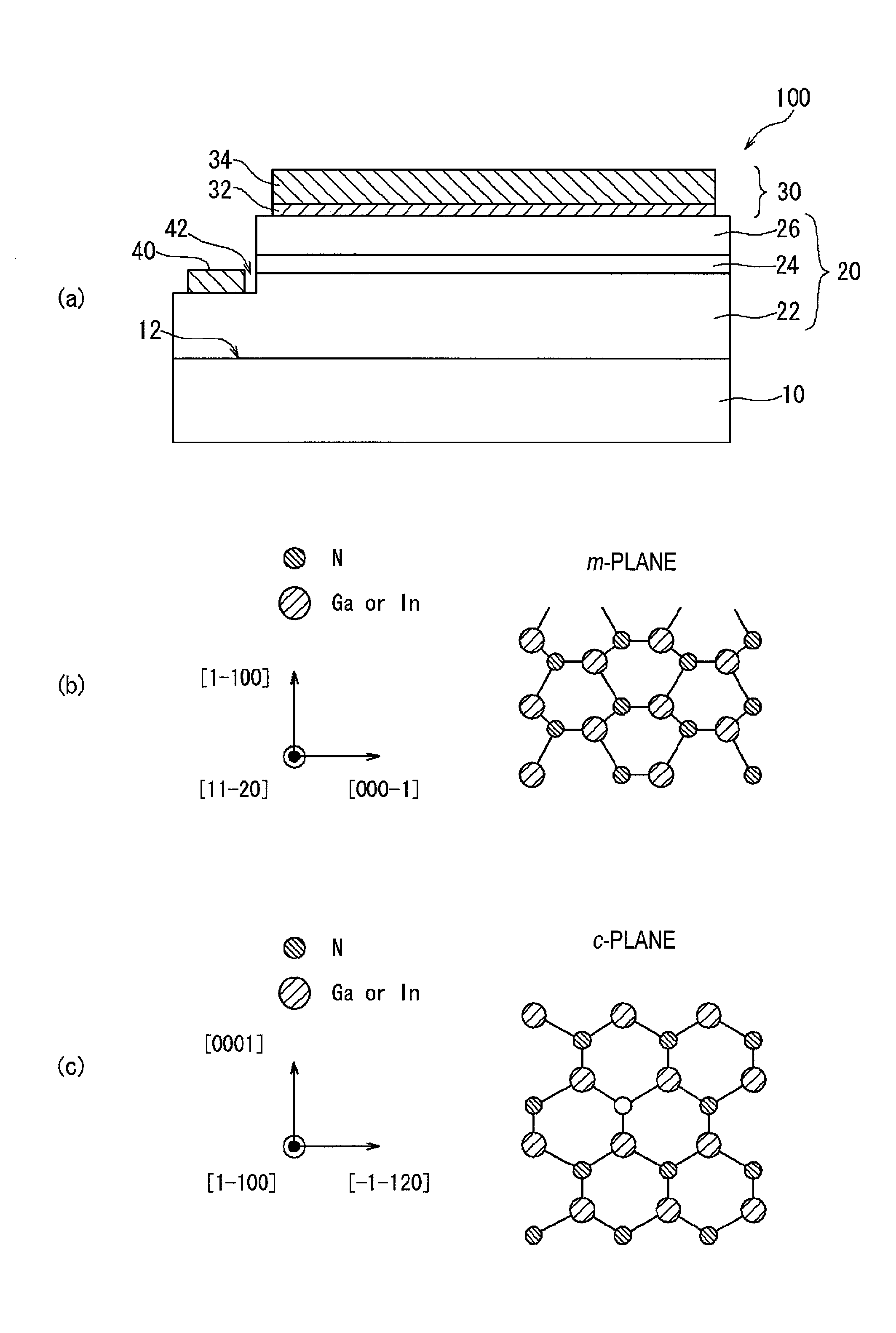
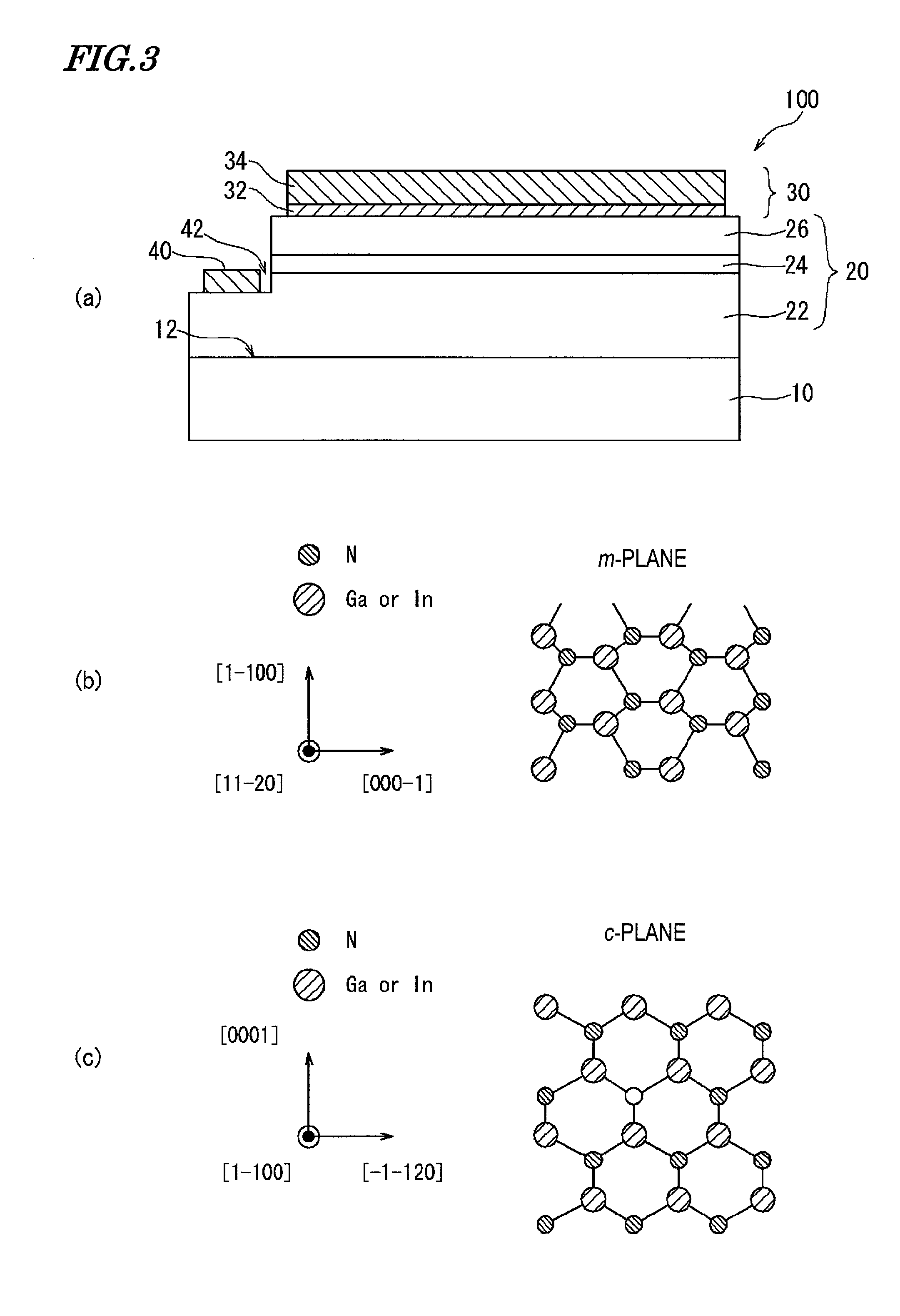
[0050]FIG. 3(a) schematically illustrates the cross-sectional structure of a nitride-based semiconductor light-emitting device 100 as a preferred embodiment of the present invention. What is illustrated in FIG. 3(a) is a semiconductor device made of GaN semiconductors and has a nitride-based semiconductor multilayer structure.
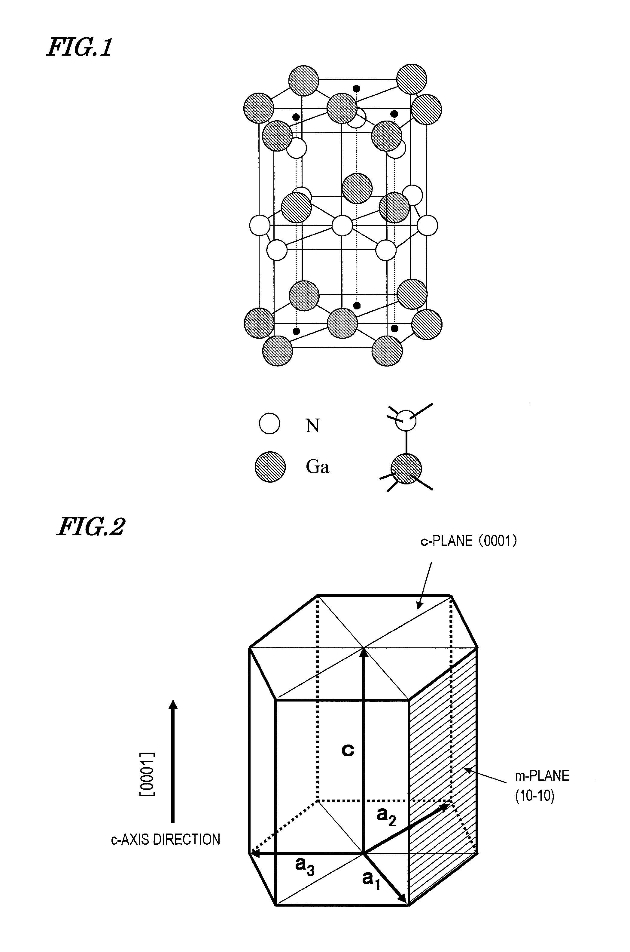
[0051]The nitride-based semiconductor light-emitting device 100 of this preferred embodiment includes a GaN-based substrate 10, of which the principal surface 12 is an m-plane, a semiconductor multilayer structure 20 that has ...
PUM
 Abstract
Description
Claims
Application Information