Frequency modulation control of a buck-boost power converter
a technology of buck-boost power converter and control circuit, which is applied in the direction of electric variable regulation, process and machine control, instruments, etc., can solve the problems of unsuitable applications, unsatisfactory user demands, and insufficient arts for some applications, so as to improve the efficiency of buck-boost power converter and reduce the switching loss of buck-boost power stag
- Summary
- Abstract
- Description
- Claims
- Application Information
AI Technical Summary
Benefits of technology
Problems solved by technology
Method used
Image
Examples
first embodiment
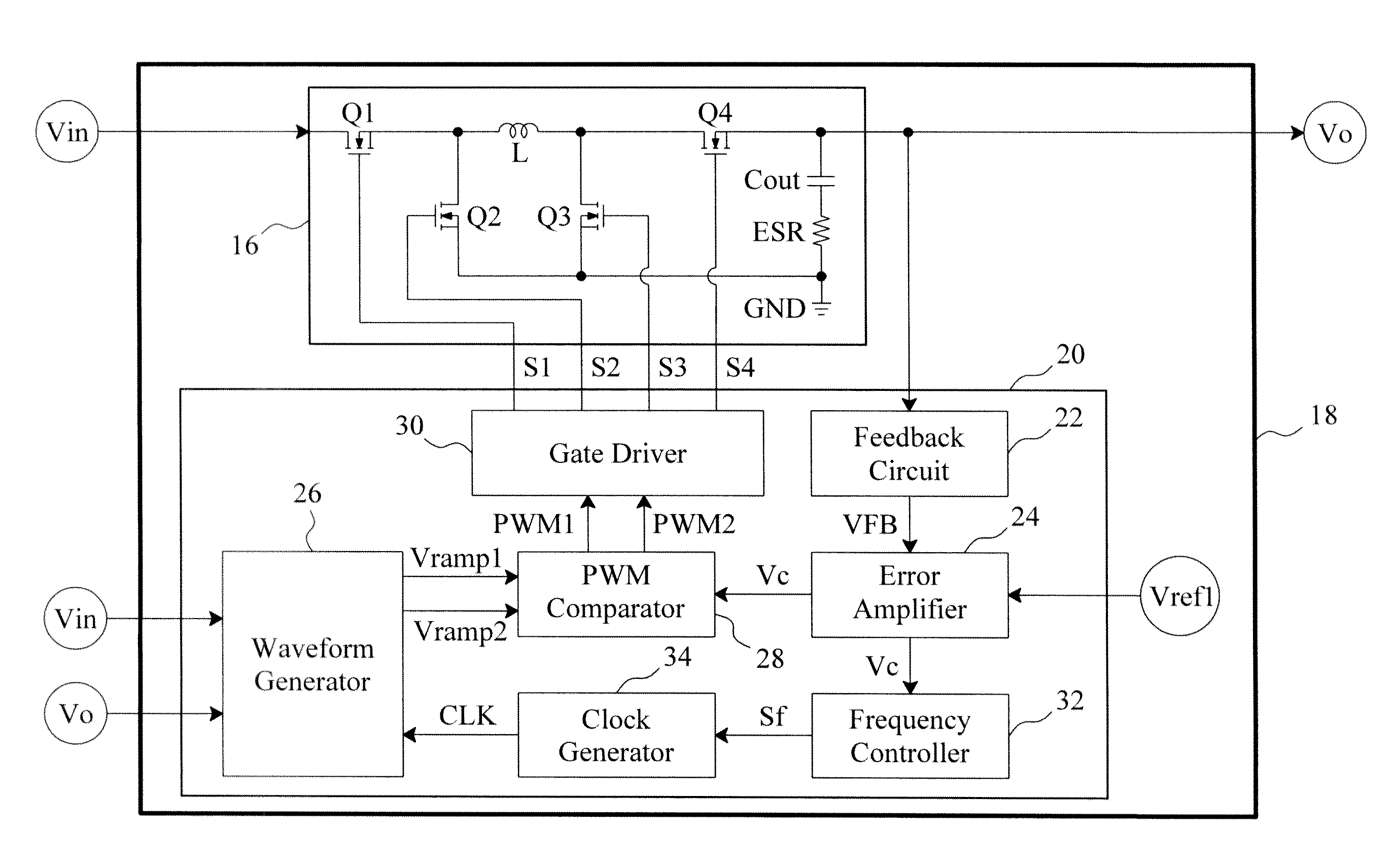
[0025]The waveform generator 26 is established by voltage sources, resistors and capacitors, and by use of the input voltage Vin and the output voltage Vo, or other signals related to the input voltage Vin and the output voltage Vo instead, controls the peaks and valleys of the ramp signals Vramp1 and Vramp2. FIG. 6 is a circuit diagram of a first embodiment for the waveform generator 26, in which a resistor R1 and a switch Q5 are connected in series between a variable voltage source Vref2 and a capacitor C, a switch Q6 is connected in parallel with the capacitor C, signals S5 and S6 control the switches Q5 and Q6, respectively, to charge and discharge the capacitor C to generate the ramp signal Vramp1, a variable voltage source Vref3 is connected between the capacitor C and a ground GND, a comparator 36 compares the ramp signal Vramp1 with a voltage Vref4 to generate a comparison signal Sc, an SR flip-flop 38 generates the signals S5 and S6 according to the clock CLK and the compar...
second embodiment
[0028]As shown in FIGS. 7 and 8, the waveform generator 26 provides a non-linear ramp signal Vramp1, which enables the buck-boost power converter 18 with better voltage regulation and transient response for heavy loading, as compared with a linear ramp signal. In addition to the waveforms shown in FIGS. 7 and 8, the waveform generator 26 may provide a non-linear ramp signal Vramp1 with other waveforms, for example, shown in FIG. 9, 10 or 11, by using different circuits and methods. FIG. 12 is a circuit diagram of a second embodiment for the waveform generator 26 to provide the ramp signal Vramp1 shown in FIG. 10, in which a resistor R2 is additionally connected in series with the switch Q6 as compared with the waveform generator 26 of FIG. 6. Due to the resistor R2, the ramp signal Vramp1 decreases to the level of the voltage Vref3 mildly when the capacitor C discharges, as shown in FIG. 10.
[0029]The circuit for generating the ramp signal Vramp2 is similar to that for generating the...
PUM
 Abstract
Description
Claims
Application Information


