Light emitting device and method for manufacturing same, lighting fixture, and lighting system

a technology of light emitting devices and manufacturing methods, which is applied in the manufacture of electrode systems, lighting support devices, vessels or leading-in conductors, etc., and can solve the problems of not meeting the requirements of high luminance and optical performan

Inactive Publication Date: 2011-02-10
HARISON TOSHIBA LIGHTING CORP +1
View PDF11 Cites 63 Cited by
  • Summary
  • Abstract
  • Description
  • Claims
  • Application Information

AI Technical Summary

Benefits of technology

[0014]According to still another aspect of the invention, there is provided a method for manufacturing a light emitting device, including: forming a electrode pattern, a groove-like light guide, and a separation groove on a wafer-like substrate; mounting a light emitting element to the substrate to electrically connect an electrode of the light emitting element and the electrode pattern, emission light of the light emitting element being capable of being introduced into the light guide; forming a phosphor-mixed layer on a first major surface of a transparent substrate and providing a lens on a second major surface side of the transparent substrate opposite to the first major surface; laminating the substrate to the first major surface side of the transparent substrate to make the light guide opposite to the phosphor-mixed layer; and cutting and separating the substrate and the transparent substrate along the separation groove.

Problems solved by technology

Thus, this example does not sufficiently satisfy the requirements of high luminance and optical system downsizing at the same time.

Method used


Image

  • Light emitting device and method for manufacturing same, lighting fixture, and lighting system
  • Light emitting device and method for manufacturing same, lighting fixture, and lighting system
  • Light emitting device and method for manufacturing same, lighting fixture, and lighting system

Examples


first embodiment

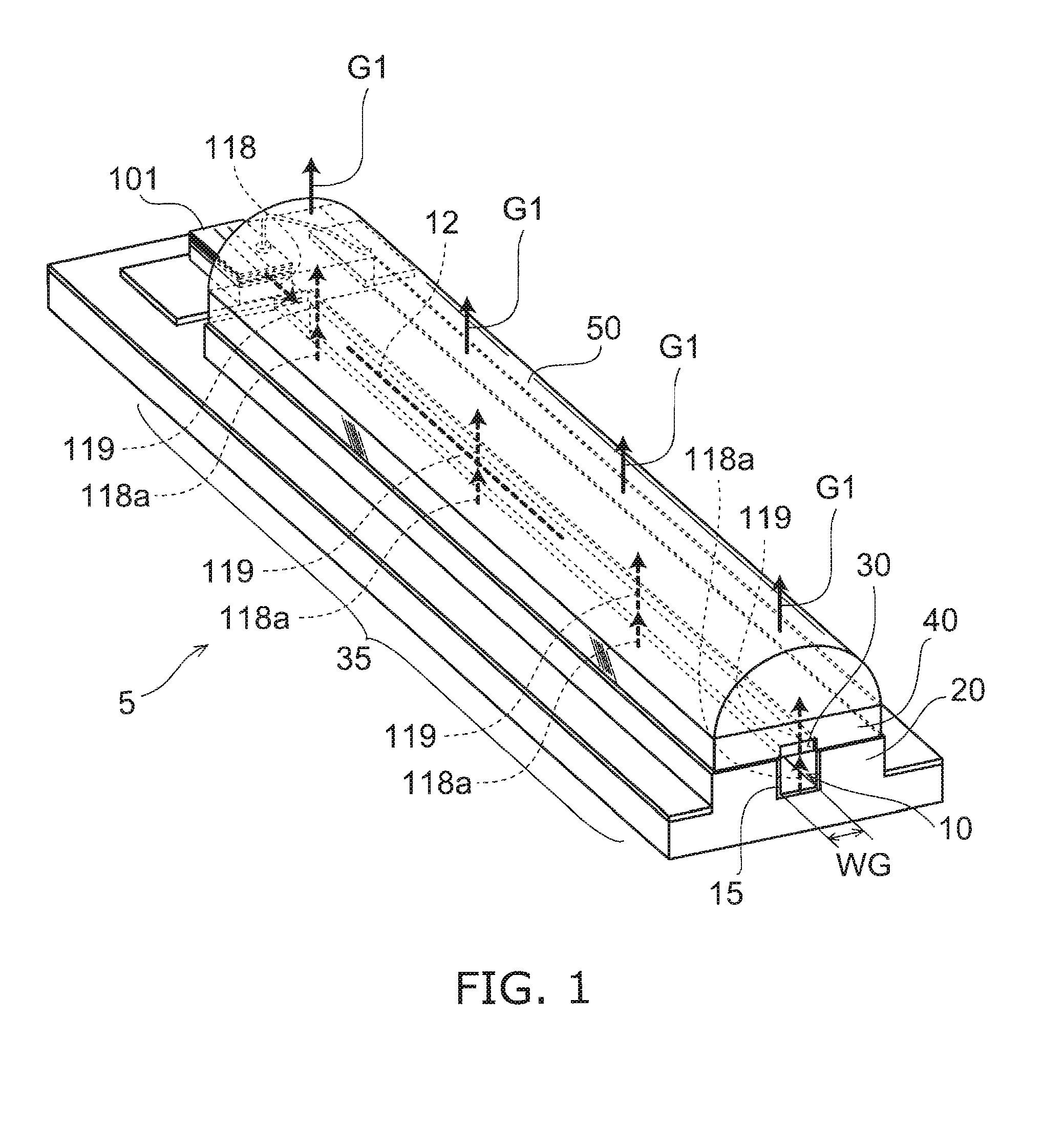
[0028]FIG. 1 is a schematic perspective view of a light emitting device according to the invention.

[0029]A light emitting device 5 includes a substrate 20 including a light guide 10 provided like a groove along a first direction 12, a light emitting element 101, and a lens 50 provided above the light guide 10.

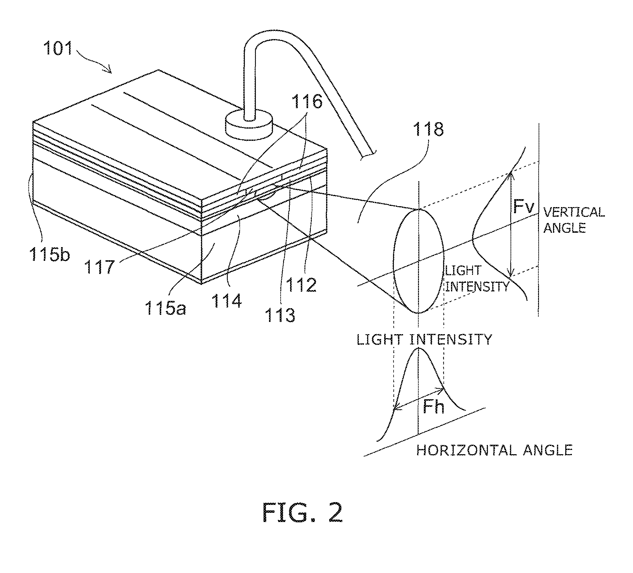
[0030]The emission light 118 from the light emitting element 101 is introduced into one end portion of the light guide 10. While spreading along the first direction 12, the introduced emission light 118 is reflected by the inner wall surface (side surface and / or bottom surface) of the light guide 10 and turned into upward light 118a directed upward above the substrate 20. The lens 50 is provided above the light guide 10 and can control light distribution characteristics in the plane generally perpendicular to the first direction 12 by collecting the upward light 118a. It is noted that the structure of the light emitting device 5 excluding the light emitting element 101 is herei...

second embodiment

[0061]FIG. 8 is a schematic perspective view of a light emitting device according to a

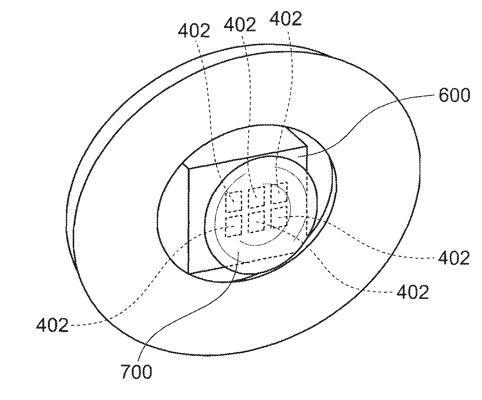
[0062]This embodiment includes two or more light emitting elements and an optical combiner 70 such as an optical waveguide coupler. In FIG. 8, three light emitting elements 101, 102, and 103 are provided. The emission lights therefrom are combined by the optical combiner 70 and then injected into the light guide 10. If the three light emitting elements 101, 102, and 103 have a generally equal wavelength, the optical output can be increased, and higher brightness can be achieved.

[0063]FIG. 9 shows a variation of the second embodiment.

[0064]Light emitting elements 81, 82, and 83 are mounted respectively on external mounting members. The outputs thereof are injected into the optical combiner 70 respectively through optical fibers 91, 92, and 93 and the like. For instance, if the three light emitting elements 81, 82, and 83 emit red, green, and blue light, respectively, then a mixed color is generated ...

third embodiment

[0065]FIG. 10 is a schematic cross-sectional view of a lighting fixture according to a

[0066]The outgoing light G1 from the light emitting device 5 is introduced from a side surface 513a of a light guide plate 513. An optical film stack 800 is provided on the upper surface 513c of the light guide plate 513. The incident light is reflected at the lower surface 513b of the light guide plate 513, and then part of it is introduced and diffused into the optical film stack 800, and then emitted upward. Part of the remaining light is reflected and further travels toward the other side surface of the light guide plate 513. By thus repeating reflection, the entire surface of the optical film stack 800 can be irradiated generally uniformly. For instance, if the width WG of the light emitting section is 100 μm or less, the light distribution angle can be narrowed despite downsizing the lens, which facilitates improving the efficiency of light extraction from the light guide plate 513. Furthermo...


PUM


Abstract

A light emitting device includes: a light emitting element; a substrate including a groove-like light guide extending along a first direction, emission light emitted from the light emitting element and introduced into the light guide being reflected by an inner wall surface of the light guide, spreading along the first direction, and being turned into upward light directed upward above the substrate; and a lens provided above the light guide and configured to collect the upward light and control light distribution characteristic in a plane generally perpendicular to the first direction.

Description

CROSS-REFERENCE TO RELATED APPLICATIONS[0001]This application is based upon and claims the benefit of priority from the prior Japanese Patent Application No. 2009-186068, filed on Aug. 10, 2009; the entire contents of which are incorporated herein by reference.BACKGROUND[0002]1. Field[0003]Embodiments of the invention relate generally to a light emitting device and a method for manufacturing the same, a lighting fixture, and a lighting system.[0004]2. Background Art[0005]Use of semiconductor light emitting elements in light emitting devices and lighting fixtures facilitates energy saving, lifetime extension, downsizing, and weight saving. Furthermore, it is also desirable to the environment because of no use of mercury and the like.[0006]Therefore, there are increasing demands for small size, low profile, and light weight in applications such as headlights and other illumination devices and backlights of liquid crystal display devices.[0007]JP-A 2006-106212 (Kokai) discloses an exam...

Claims


Application Information

Patent Timeline
Patent Type & Authority Applications(United States)
IPC IPC(8): F21V8/00F21V7/04H01J9/00F21V9/40
CPCF21K9/56F21V9/16F21Y2101/02F21Y2101/025G02B19/0061G02B6/0096G02B27/0966G02B27/0994G02B19/0028G02B6/0053F21V13/14F21K9/64F21Y2115/10F21Y2115/30F21V9/32H01L2224/48091H01L2924/00014F21V9/30
Inventor KINOSHITA, JUNICHI
Owner HARISON TOSHIBA LIGHTING CORP
Why Eureka
Try Eureka