

Lateral emission LED backlight for LCD
- Summary
- Abstract
- Description
- Claims
- Application Information
AI Technical Summary
Benefits of technology
Problems solved by technology
Method used
Image

Examples
embodiment 1
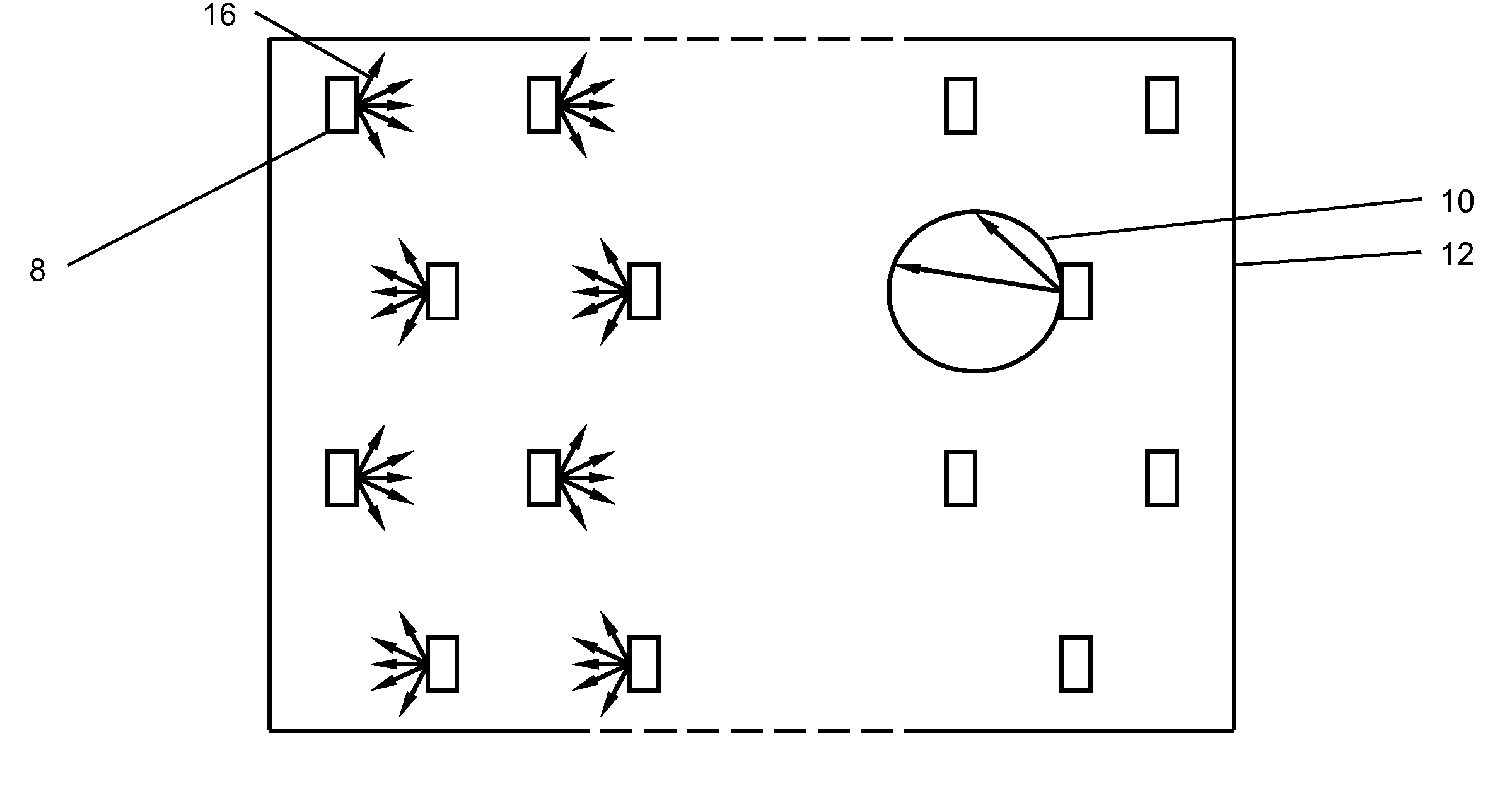
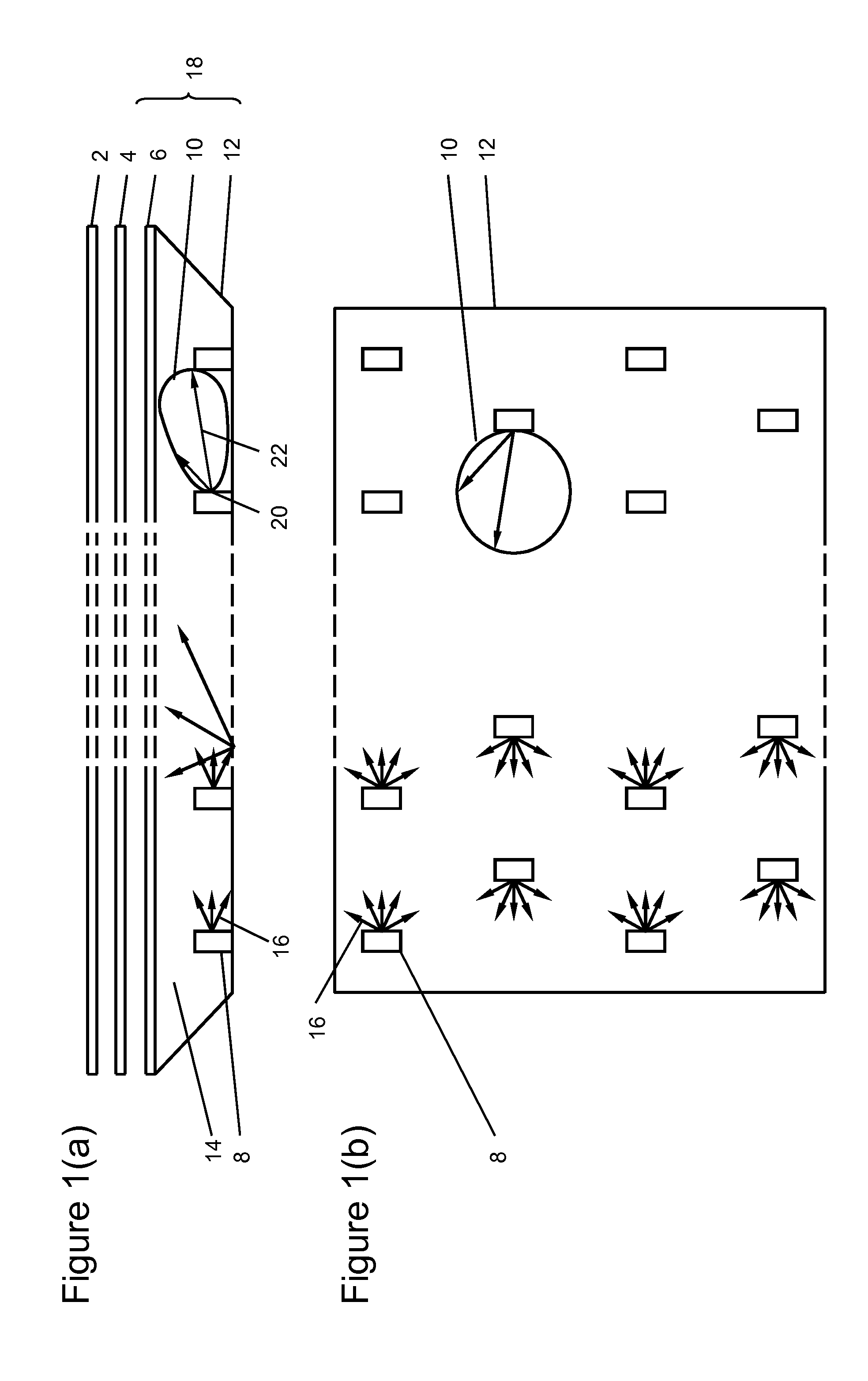
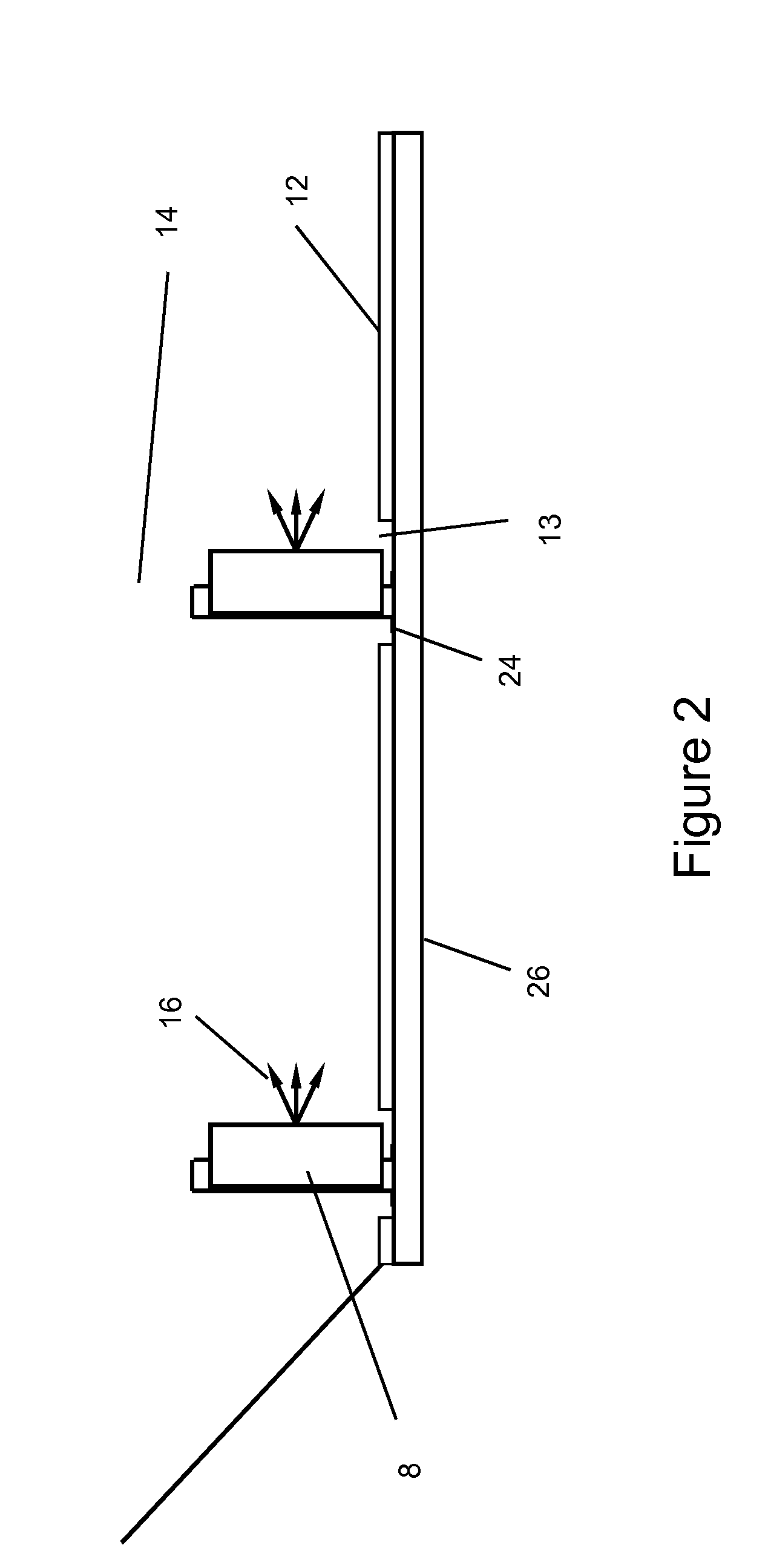
[0063]FIG. 1(a) shows a cross-section of a backlight unit 18, comprising LEDs 8, arranged in a regular array, a reflector 12, a light diffusion plate 6, and a cavity 14. The LEDs 8 are placed above a reflector 12. Some distance above the reflector 12 there is a diffuser 6, the purpose of which is to homogenise the light emitted by the LEDs 8; the diffuser may also provide some beam shaping functions, for example by the inclusion of optical features such as may be found on Brightness Enhancement Films (BEFs). Above the diffuser 6 is placed a Liquid Crystal Display (LCD) panel 2 that is to be illuminated by the backlight unit 18. Additional films 4 may be placed between the backlight unit 18 and the LCD 2. The function of these films 4 is to provide further light shaping of the light emitted by the backlight unit 18. The films may comprise BEFs, light shaping diffusers, and reflective polarisers such as the Dual Brightness Enhancement Film (DBEF), made by 3M.
[0064]The LEDs 8 are posit...
embodiment 2
[0070]In this embodiment the LEDs 8 used have a Lambertian emission profile. Despite not having an emission profile which has been modified as described hereinbefore, it is possible to reduce the thickness of the backlight cavity 14, yet maintaining good spatial uniformity of light at the diffuser, 6. The LEDs 8 are arranged as described above, but now the package is rotated slightly towards the rear reflector 12 as shown in FIGS. 3(a) and 3(b). The polar emission profile 10 now has a shape that is circular (before it intersects with any of the other components of the backlight unit). The effect of rotating the package so that the primary emission direction (normal to the emitting area 20) is at an angle of 95 degrees to 140 degrees from normal to the display panel 2, and preferably 100 degrees to 120 degrees, is that more light is directed back towards the reflector 12 and less light directly illuminates the diffuser 6. Consequently, the light path of the light emitted by the LEDs ...
embodiment 3
[0073]As mentioned hereinbefore, the emission profile of the LED 8 may be made asymmetric through the use of photonic structures either formed in the LED chip itself, or in an over-layer that is adhered to the chip during manufacture. The emission profile of the LED 8 may be modified in one direction only, for example, through the use of a 1-dimensional diffraction grating which has been imprinted into the semiconductor material. This is schematically shown in FIG. 4, which shows an exemplary LED 8 including a package 36 and an LED chip 38. The LED chip 38 includes a substrate 28, multi-quantum well region 32, n-type or p-type region 30, and p-type or n-type region 34, in which a photonic structure 40, has been formed. Alternatively, the photonic structure 40 could be imprinted into an overlayer, for example, a photoresist material which has been coated onto the LED chip 38, or an encapsulant that is used to seal the LED package.
[0074]In one example, a diffraction grating with a pit...
PUM
 Abstract
Description
Claims
Application Information