Substrate for light emitting diode package and light emitting diode package having the same

a technology of light emitting diodes and substrates, which is applied in the manufacture of semiconductor/solid-state devices, electrical devices, semiconductors, etc., can solve the problems of small amount of heat released through the board, poor heat release characteristics of pcb made of plastic materials, and large heat generation of light emitting diodes and electronic elements. , to achieve the effect of high heat release properties, high reflexibility and high luminan

Inactive Publication Date: 2011-02-24
SAMSUNG ELECTRO MECHANICS CO LTD
View PDF12 Cites 69 Cited by
  • Summary
  • Abstract
  • Description
  • Claims
  • Application Information

AI Technical Summary

Benefits of technology

[0011]An aspect of the present invention provides a metal substrate for a light emitting diode (LED) package having high heat release properties, high luminance, and high reflexibility, and an LED package having the same.

Problems solved by technology

In general, light emitting diodes and electronic elements generate a great deal of heat when operated due to internal resistance or the like.
However, as it is difficult for a single light emitting diode chip to have such a high level of luminance, a plurality of light emitting diode arrays are commonly configured to obtain the required level of luminance.
The PCB made of a plastic material does not have good heat release characteristics, so a relatively small amount of heat is released through the board.
Thus, when an element generating excessive heat is mounted on the board, because its heat is not properly released, the element malfunctions or its life span is shortened.
Although the metal core PCB has good heat release characteristics when compared with the general PCB made of a plastic material, its fabrication cost is high because it uses high-priced polymer having a relatively high thermal conductivity.
In addition, its reflexibility and heat release characteristics are degraded by the polymer insulation layer.

Method used


Image

  • Substrate for light emitting diode package and light emitting diode package having the same
  • Substrate for light emitting diode package and light emitting diode package having the same
  • Substrate for light emitting diode package and light emitting diode package having the same

Examples


Embodiment Construction

[0033]Exemplary embodiments of the present invention will now be described in detail with reference to the accompanying drawings. The invention may, however, be embodied in many different forms and should not be construed as being limited to the embodiments set forth herein. Rather, these embodiments are provided so that this disclosure will be thorough and complete, and will fully convey the scope of the invention to those skilled in the art. In the drawings, the shapes and dimensions may be exaggerated for clarity, and the same reference numerals will be used throughout to designate the same or like components.

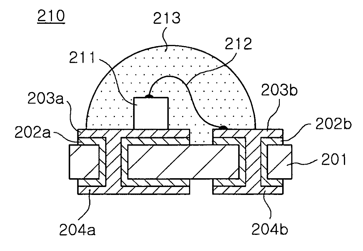
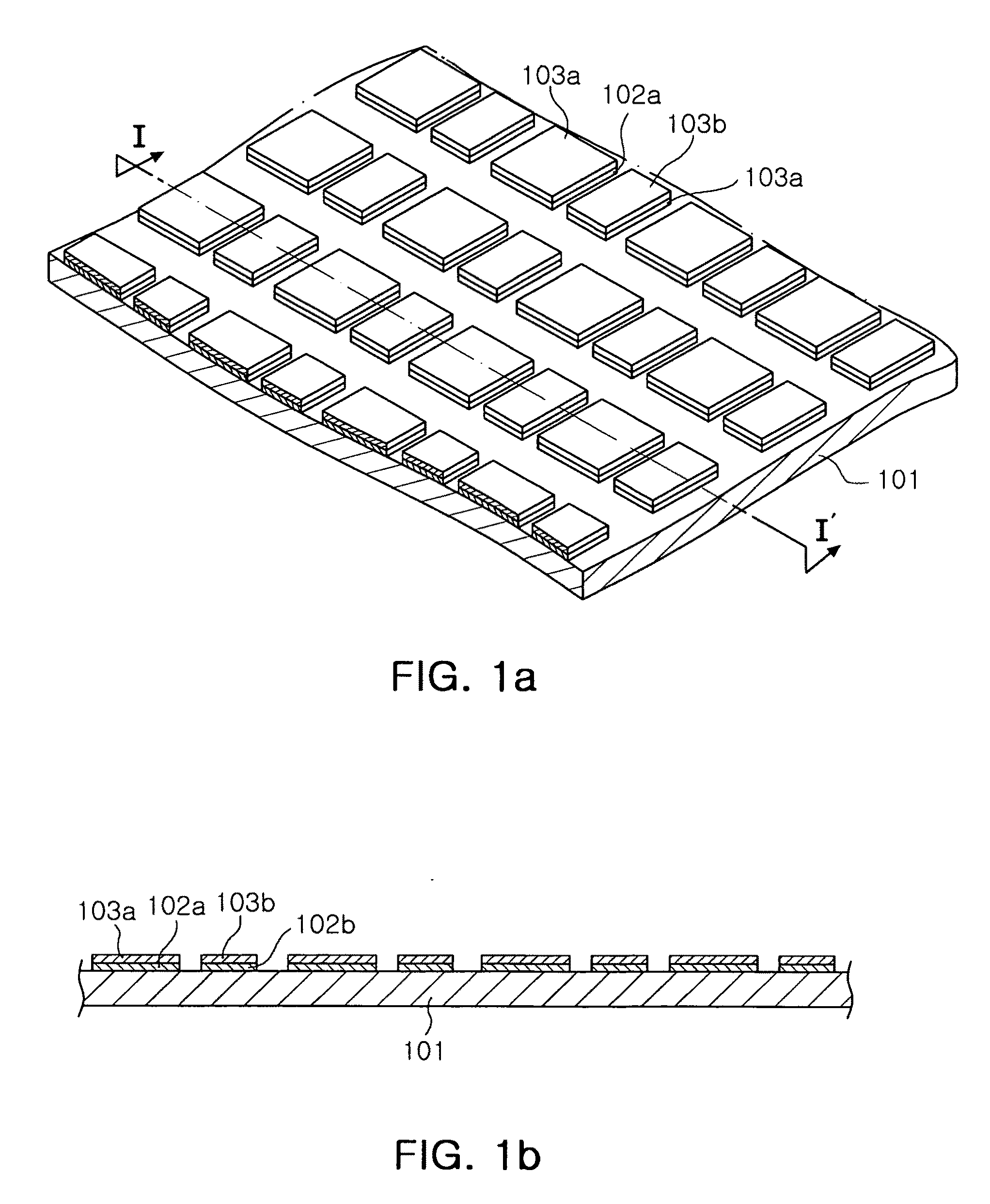
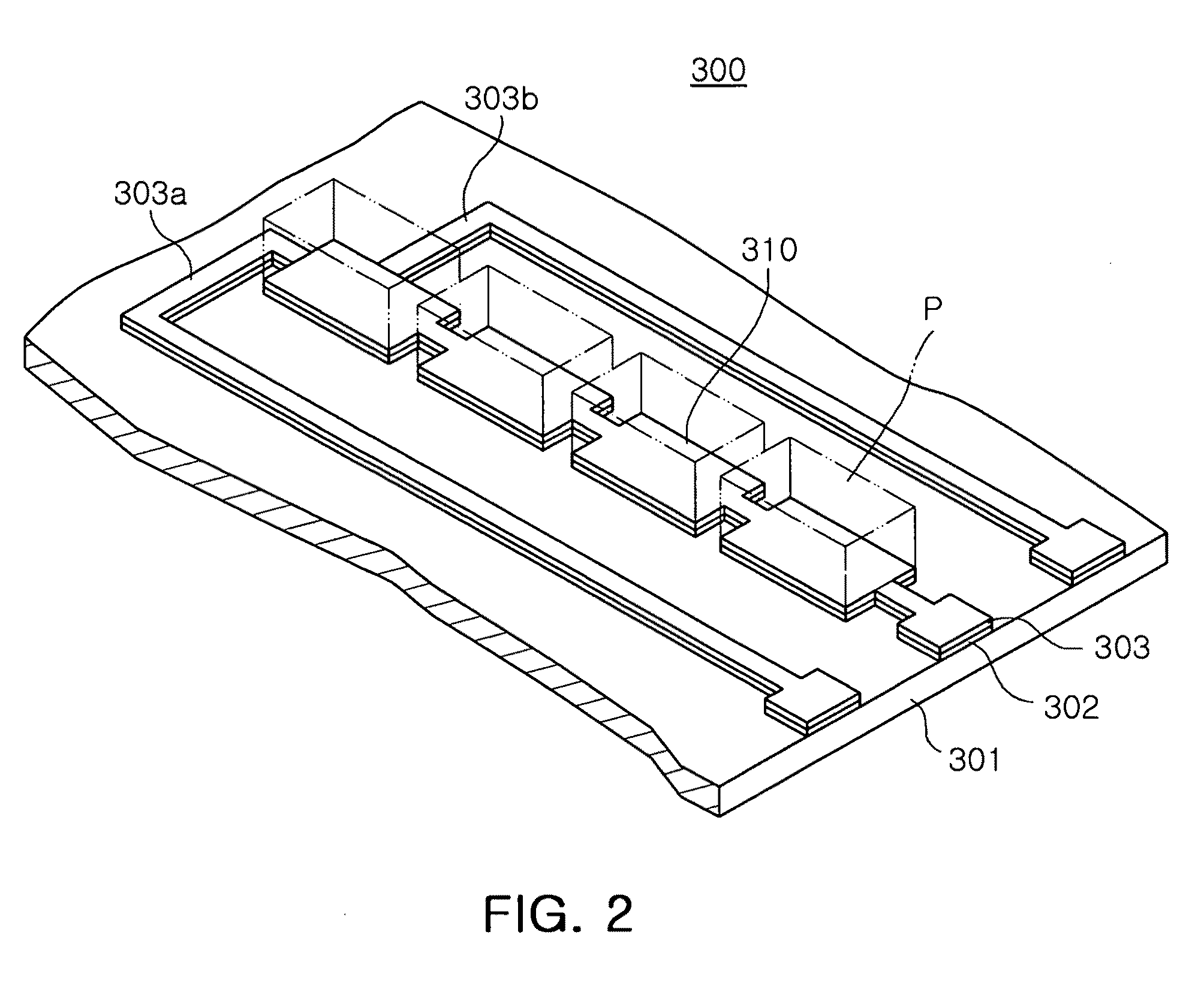
[0034]FIG. 1a is a perspective view of a metal substrate according to an exemplary embodiment of the present invention, and FIG. 1b is a sectional view taken along line I-I′ of FIG. 1.

[0035]With reference to FIGS. 1a and 1b, the metal substrate includes a metal plate 101, insulation oxide layers 102a and 102b formed on portions of the surface of the metal plate 101, a first ...


PUM


Abstract

A substrate for a light emitting diode (LED) package, and an LED package having the same are disclosed. The substrate for an LED package includes: a metal plate; an insulation oxide layer formed on a portion of the surface of the metal plate; a first conductive pattern formed at one region of the insulation oxide layer and providing a light emitting diode mounting area; and a second conductive pattern formed at another region of the insulation oxide layer such that it is separated from the first conductive pattern. In the substrate for an LED package, because regions of the insulation oxide layer other than regions for insulating conductive patterns are removed, heat generated from the light emitting diode can be effectively released. In addition, degradation of reflexibility and luminance of the LED due to the insulation oxide layer can be prevented.

Description

CROSS-REFERENCE TO RELATED APPLICATIONS[0001]This application claims the priority of Korean Patent Application No. 10-2009-0078403 filed on Aug. 24, 2009, in the Korean Intellectual Property Office, the disclosure of which is incorporated herein by reference.BACKGROUND OF THE INVENTION[0002]1. Field of the Invention[0003]The present invention relates to a metal substrate for a light emitting diode package and a light emitting diode package having the same and, more particularly, to a metal substrate for a light emitting diode package having high heat release properties, high luminance, and high reflexibility, and a light emitting diode package having the same.[0004]2. Description of the Related Art[0005]In general, light emitting diodes and electronic elements generate a great deal of heat when operated due to internal resistance or the like. A computer CPU is a typical element generating heat, and a dedicated cooling element is added to such an element generating strong heat to a p...

Claims


Application Information

Patent Timeline
Patent Type & Authority Applications(United States)
IPC IPC(8): H01L33/00
CPCH01L33/486H01L33/60H01L2924/12041H01L2224/4848H01L2924/01322H01L2224/48227H01L2224/48091H01L24/97H01L33/647H01L2924/00014H01L2924/00H01L2224/48465
Inventor PARK, SUNG KEUNCHOI, SEOG MOONSOHN, YOUNG HOKIM, TAE HYUNLEE, YOUNG KI
Owner SAMSUNG ELECTRO MECHANICS CO LTD
Why Eureka
Try Eureka