Photovoltaic device and method for manufacturing the same

a photovoltaic device and photovoltaic technology, applied in the field of photovoltaic devices, can solve the problems of short supply the inability of solar-grade silicon wafers to meet the explosive demand, and the inability to meet the demand etc., to reduce the manufacturing cost of photovoltaic devices. , the problem of shortage of solar-grade silicon wafers

a photovoltaic device and photovoltaic technology, applied in the field of photovoltaic devices, can solve the problems of short supply the inability of solar-grade silicon wafers to meet the explosive demand, and the inability to meet the demand etc., to reduce the manufacturing cost of photovoltaic devices. , the problem of shortage of solar-grade silicon wafers

US20110048499A1Inactive Publication Date: 2011-03-03INTELLECTUAL DISCOVERY CO LTD

Image

  • Photovoltaic device and method for manufacturing the same
  • Photovoltaic device and method for manufacturing the same
  • Photovoltaic device and method for manufacturing the same

Examples


Embodiment Construction

[0017]A photovoltaic device according to an embodiment of the present invention and a method for manufacturing the photovoltaic device will be described with reference to the drawings.

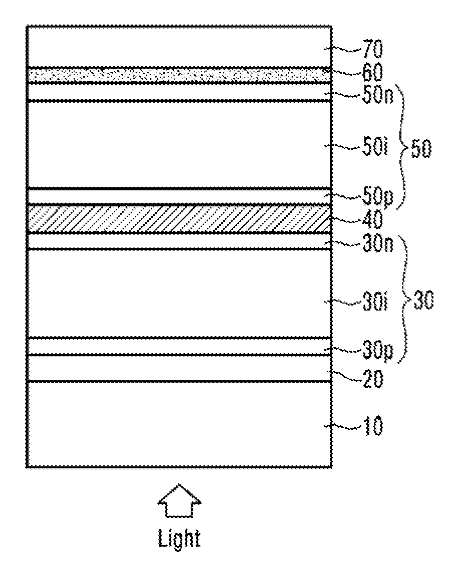
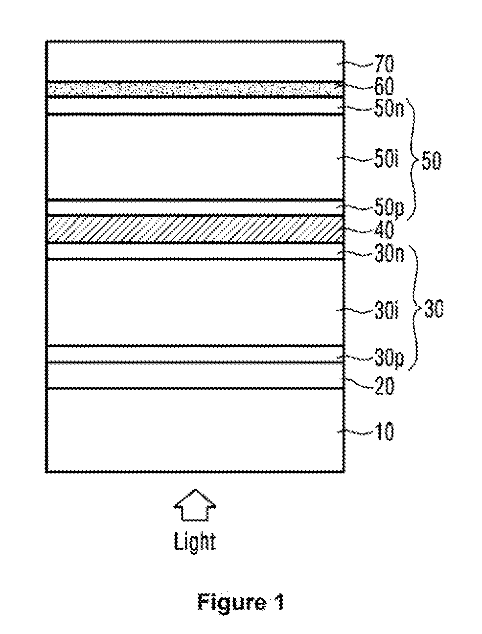
[0018]A photovoltaic device may have a double junction structure and a triple junction structure and the like. In FIG. 1, a photovoltaic device having the double junction structure will be described as an example.

[0019]As shown in FIG. 1, a photovoltaic device according to an embodiment of the present invention includes a substrate 10, a first electrode 20, a first unit cell 30, an intermediate reflector 40, a second unit cell 50 and a second electrode 70. In the embodiment of the present invention, the substrate 10 may include an insulating transparent material such as glass.

[0020]The first electrode 20 is formed on the substrate 10 and may include transparent conducting oxide (TCO) such as ZnO.

[0021]The first unit cell 30 is placed on the first electrode 20. The first unit cell 30 includes a p-type w...


PUM


Abstract

Disclosed is a photovoltaic device. The photovoltaic device includes a substrate; a first unit cell disposed on the substrate and comprising a p-type window layer, an i-type photoelectric conversion layer and an n-type layer; an intermediate reflector disposed on the first unit cell and comprising a hydrogenated n-type microcrystalline silicon carbide or a hydrogenated n-type microcrystalline silicon nitride profiled such that carbon concentration or nitride concentration is higher the farther it is from a light incident side; and a second unit cell disposed on the intermediate reflector and comprising a p-type window layer, an i-type photoelectric conversion layer and an n-type layer.

Description

CROSS-REFERENCE TO RELATED APPLICATION[0001]This application claims the benefit of Korean Patent Application No. 10-2009-0082355 filed on Sep. 2, 2009, the entirety of which is hereby incorporated by reference.FIELD OF THE INVENTION[0002]This embodiment relates to a photovoltaic device and a method for manufacturing the same.BACKGROUND OF THE INVENTION[0003]Recently, because of high oil prices and the global warming phenomenon based on a large amount of CO2 emissions, energy is becoming the most important issue in determining the future life of mankind. Even though many technologies using renewable energy sources including wind force, bio-fuels, hydrogen / fuel cells and the like have been developed, a photovoltaic device using sunlight is in the spotlight. This is because solar energy, the origin of all energies, is an almost infinite clean energy source.[0004]The sunlight incident on the surface of the earth has an electric power of 120,000 TW. Thus, theoretically, a photovoltaic de...

Claims


Application Information

Patent Timeline
03 Mar 2011
Publication
US20110048499A1
IPC
H01L31/0232; H01L31/18; H01L31/076
CPC
H01L31/076; Y02E10/52; H01L31/0549; H01L31/056; Y02E10/548; H01L31/047
Inventors
MYONG, SEUNG-YEOP