Hybrid Packaged Gate Controlled Semiconductor Switching Device Using GaN MESFET

a technology of gan mesfet and semiconductor, applied in the field of physical level packaging of an electrical switching circuit, can solve the problems of increasing the leakage current of the device, and achieve the effect of reducing the package footprint and larger die siz

Inactive Publication Date: 2011-03-03
ALPHA & OMEGA SEMICON INC
View PDF18 Cites 59 Cited by
  • Summary
  • Abstract
  • Description
  • Claims
  • Application Information

AI Technical Summary

Benefits of technology

[0017]As a result, the HPSD becomes a stacked package of IGT die and RGT die with reduced package footprint while allowing larger die sizes and flexible placements of device terminal electrodes on the IGT die.

Problems solved by technology

Another concern associated with the silicon-silicon carbide composite substrate is the potential of increased device leakage current due to molecular level structural defects at the silicon-silicon carbide interface.

Method used


Image

  • Hybrid Packaged Gate Controlled Semiconductor Switching Device Using GaN MESFET
  • Hybrid Packaged Gate Controlled Semiconductor Switching Device Using GaN MESFET
  • Hybrid Packaged Gate Controlled Semiconductor Switching Device Using GaN MESFET

Examples


Embodiment Construction

[0036]The description above and below plus the drawings contained herein merely focus on one or more currently preferred embodiments of the present invention and also describe some exemplary optional features and / or alternative embodiments. The description and drawings are presented for the purpose of illustration and, as such, are not limitations of the present invention. Thus, those of ordinary skill in the art would readily recognize variations, modifications, and alternatives. Such variations, modifications and alternatives should be understood to be also within the scope of the present invention.

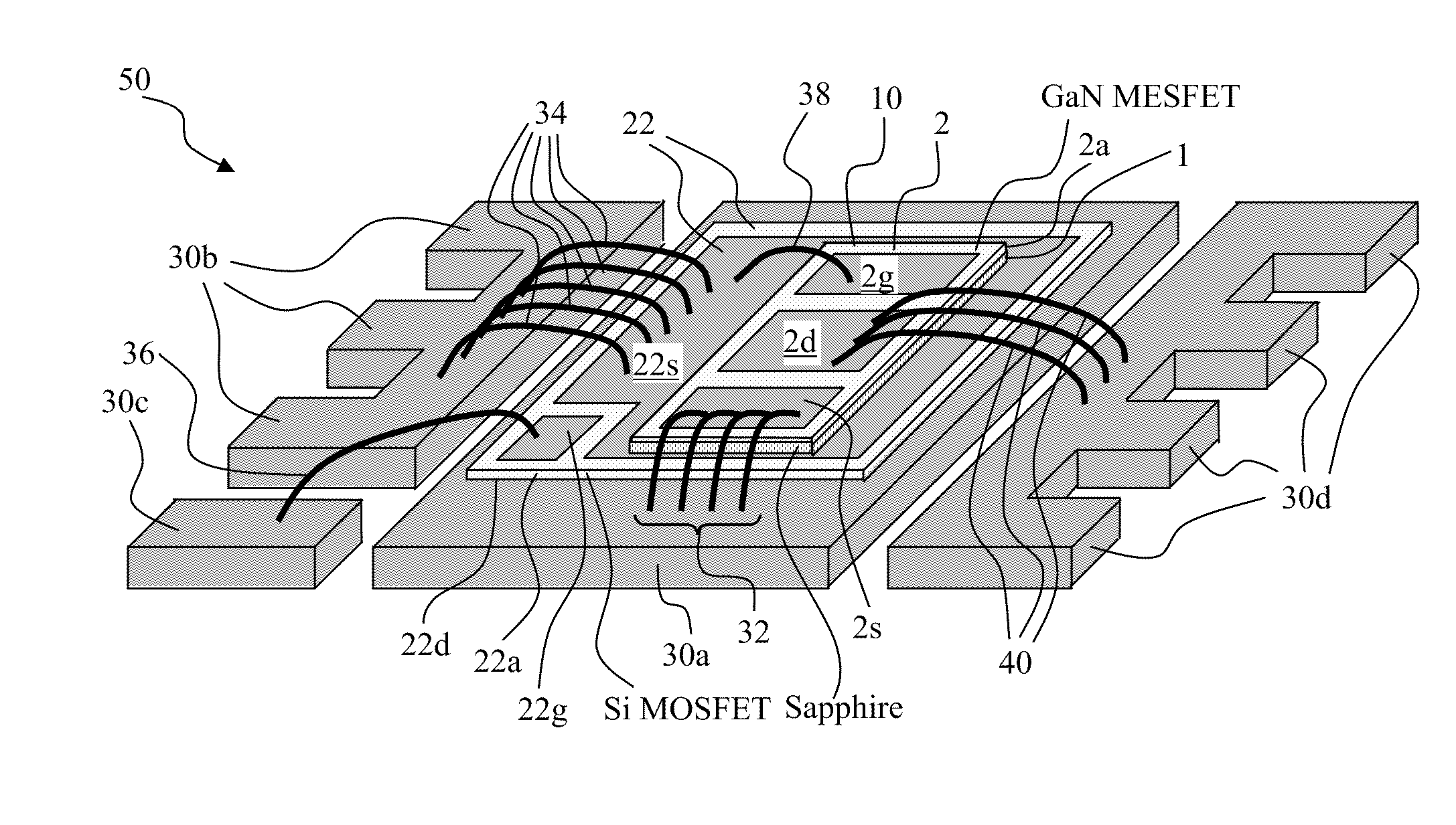
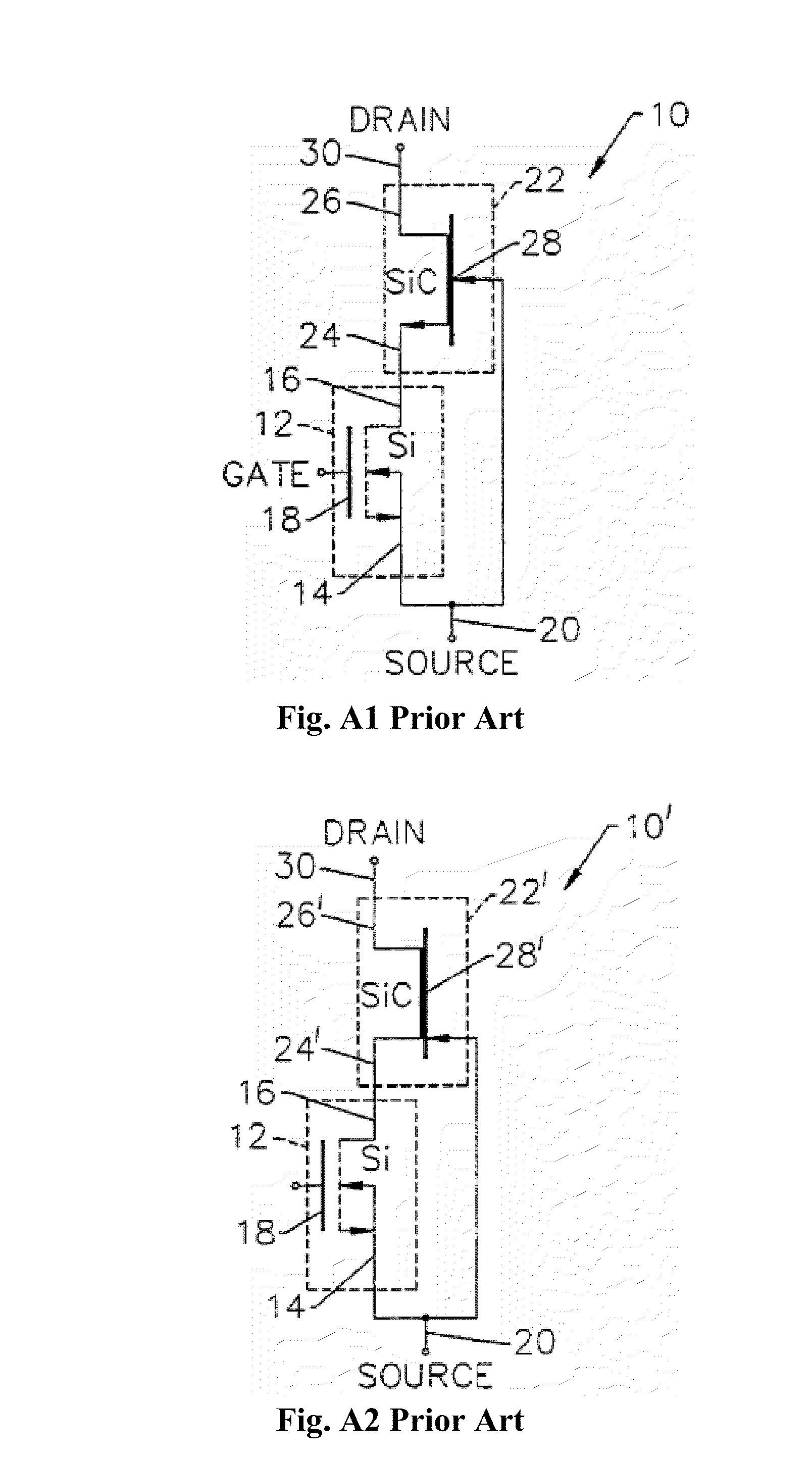
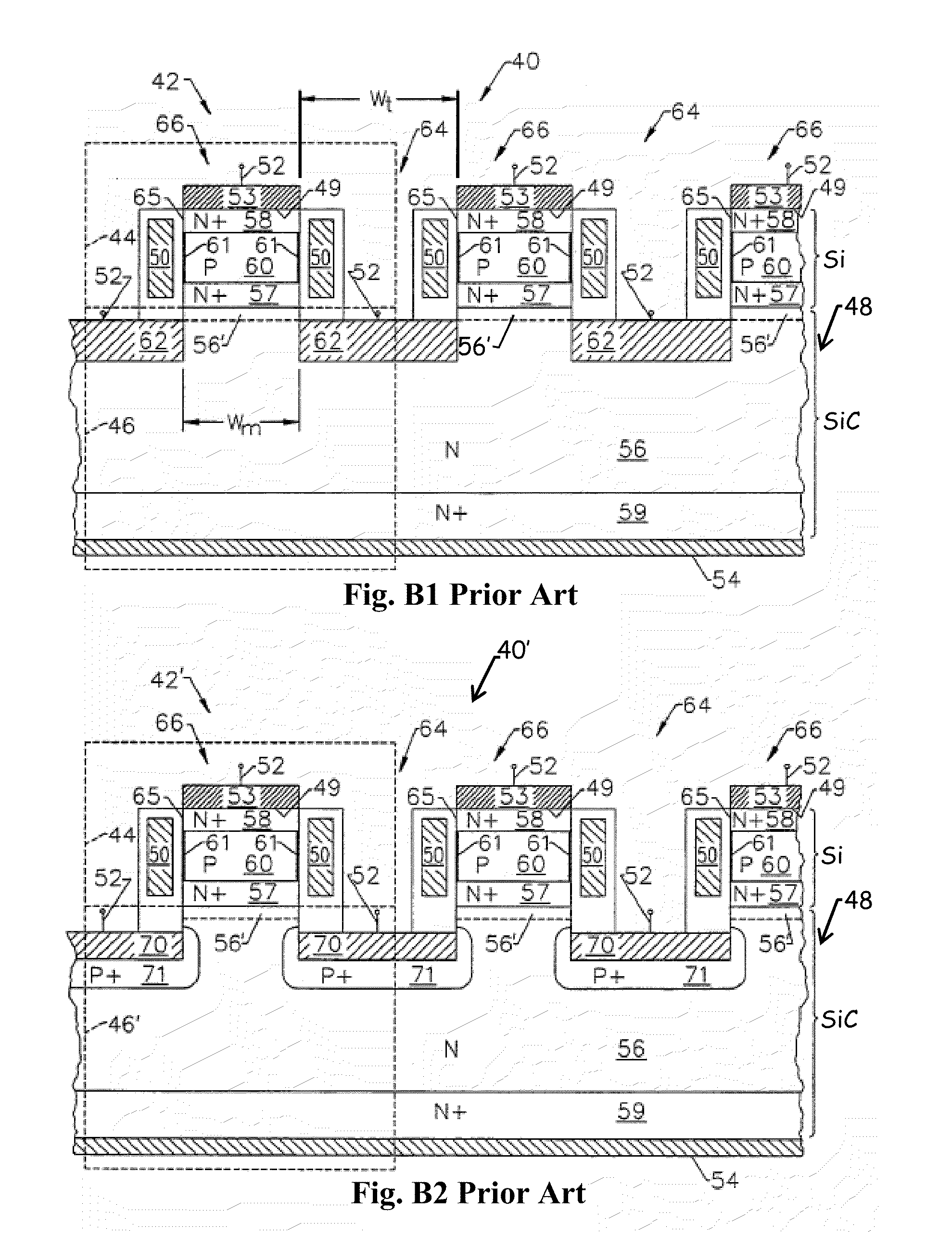
[0037]FIG. 1 together with FIG. 2A are perspective illustrations of a first device structural configuration of a hybrid packaged 3-terminal gate controlled semiconductor switching device (HPSD) 50, together with a rectifying-gate transistor (RGT) die 10, under the present invention.

[0038]The HPSD 50 has a package base that, in this case, includes numerous leadframe sections 30a, 30b, 30...


PUM


Abstract

A hybrid packaged gate controlled semiconductor switching device (HPSD) has an insulated-gate transistor (IGT) made of a first semiconductor die and a rectifying-gate transistor (RGT) made of a second semiconductor die. The RGT gate and source are electrically connected to the IGT source and drain respectively. The HPSD includes a package base with package terminals for interconnecting the HPSD to external environment. The IGT is die bonded atop the package base. The second semiconductor die is formed upon a composite semiconductor epi layer overlaying an electrically insulating substrate (EIS) thus creating a RGT die. The RGT die is stacked and bonded atop the IGT die via the EIS. The IGT, RGT die and package terminals are interconnected with bonding wires. Thus, the HPSD is a stacked package of IGT die and RGT die with reduced package footprint while allowing flexible placements of device terminal electrodes on the IGT.

Description

CROSS REFERENCE TO RELATED APPLICATIONS[0001]This application is related to the following patent applications that are incorporated herein by reference for any and all proposes:[0002]U.S. application Ser. No. 11 / 830,951 entitled “A Multi-die DC-DC Boost Power Converter with Efficient Packaging” by Francois Hebert et al with filing date of Jul. 31, 2007, hereinafter referred to as U.S. Ser. No. 11 / 830,951.[0003]U.S. application Ser. No. 11 / 830,996 entitled “A Multi-die DC-DC Buck Power Converter with Efficient Packaging” by Francois Hebert et al with filing date of Jul. 31, 2007, hereinafter referred to as U.S. Ser. No. 11 / 830,996.[0004]U.S. application Ser. No. 12 / 391,251 entitled “Compact Power Semiconductor Package and Method with Stacked Inductor and Integrated Circuit Die” by Tao Feng et al with filing date of Feb. 23, 2009, hereinafter referred to as U.S. Ser. No. 12 / 391,251.[0005]U.S. application Ser. No. 12 / 397,473 entitled “Compact Inductive Power Electronics Package” by Tao...

Claims


Application Information

Patent Timeline
Patent Type & Authority Applications(United States)
IPC IPC(8): H01L27/088H01L21/98H01L23/52
CPCH01L23/49575H01L25/50H01L2924/13062H01L2924/30107H01L2224/49111H01L2224/48145H01L2224/48091H01L2924/13091H01L2224/48247H01L2224/48245H03K17/567H01L24/48H01L2924/00014H01L2924/00H01L2924/13063H01L2924/14H01L24/49H01L2224/0603H01L2224/48257H01L2224/45099H01L2224/45015H01L2924/207H01L2924/00012
Inventor LUI, SIKBHALLA, ANUP
Owner ALPHA & OMEGA SEMICON INC
Why Eureka
Try Eureka