Optical element module and manufacturing method thereof, electronic element module and manufacturing method thereof, and electronic information device

a technology of optical elements and manufacturing methods, applied in the direction of manufacturing tools, instruments, television systems, etc., can solve the problems of reducing or varying optical characteristics, and achieve the effect of high accuracy, favorable optical characteristics, and high accuracy

Inactive Publication Date: 2011-03-03
SHARP KK
View PDF6 Cites 21 Cited by
  • Summary
  • Abstract
  • Description
  • Claims
  • Application Information

AI Technical Summary

Benefits of technology

As a result, the slanting surface of the first lens and the slanting surface inside the light shielding holder are guided together, so that the protruded slanting surface is engaged with the concaved slanting surface. This enables, for example, to position a lens module having a first lens and a second lens with high accuracy along an engaging section of a light shielding holder. As a result, it becomes possible to prevent the misalignment and tilting of the lens optical axis C relative to the aperture opening of the light shielding holder and the center of the aperture opening to make the optical characteristics favorable.
According to the present invention described

Problems solved by technology

As a result, the space between the lenses will not be stabilized and there will be misalignment or tilting from an optical axis C to

Method used


Image

  • Optical element module and manufacturing method thereof, electronic element module and manufacturing method thereof, and electronic information device
  • Optical element module and manufacturing method thereof, electronic element module and manufacturing method thereof, and electronic information device
  • Optical element module and manufacturing method thereof, electronic element module and manufacturing method thereof, and electronic information device

Examples


embodiment 1

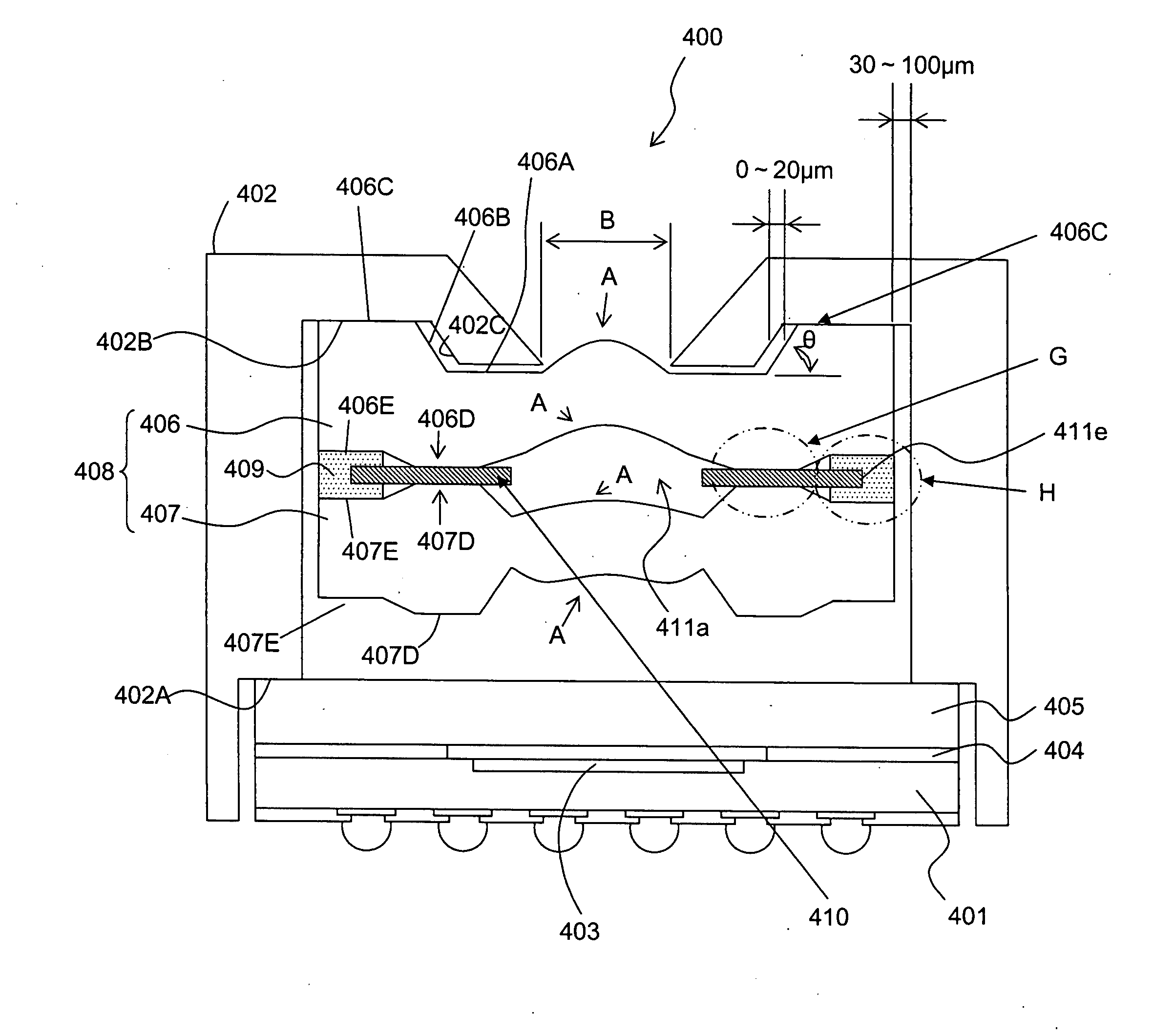
FIG. 1 is a schematic external view of an electronic element module 400 according to Embodiment 1, where FIG. 1(a) is a perspective view and FIG. 1(b) is a top view of the electronic element module 400.

As illustrated in FIGS. 1(a) and 1(b), the electronic element module 400 (sensor module 10) as the electronic element module according to Embodiment 1 includes: an optical element or an optical element module (not shown), such as one or a plurality of lenses, in which an optical surface A is provided at the center portion; and an image capturing element chip 401. The optical element or optical element module and the image capturing element chip 401 are housed within a light shielding holder 402 such that an optical surface A corresponds and aligns with an aperture opening B. By the light shielding holder 402, the top and side surfaces are covered, except the optical surface A, to shield the surface of the image capturing element from light. A plurality of the electronic element module...

embodiment 2

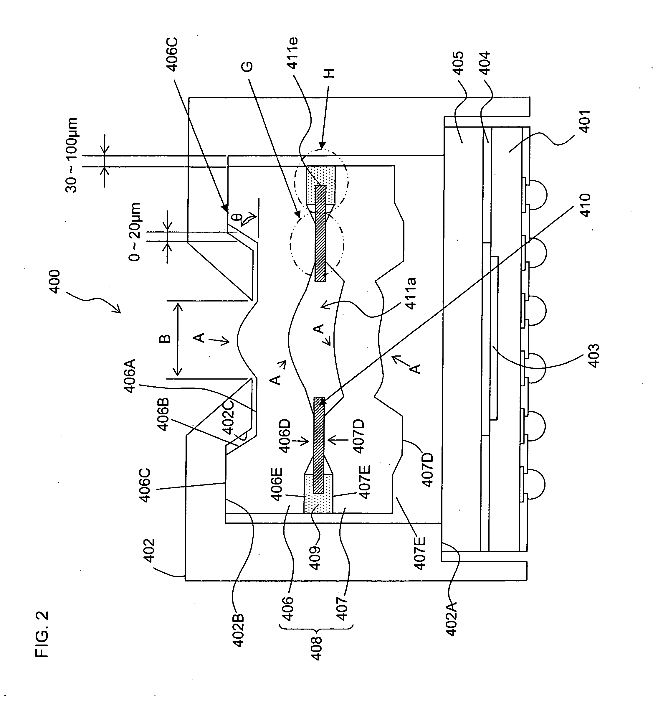
In Embodiment 1 above, described is the case where the annular slanting surface of the optical element forms a concave section and the annular slanting surface of the light shielding holder forms a convex section, that is to say, the case where the concave annular slanting surface 406B of the first lens 406 and the convex annular slanting surface 402C protruded toward the inside of the aperture opening B of the light shielding holder 402 are guided together, so that the lens module 408 and the light shielding holder 402 are positioned with high accuracy. In Embodiment 2, a case will be described where the annular slanting surface of the optical element forms a convex section, and the annular slanting surface of the light shielding holder forms a concave section, that is to say, a case where the first lens side includes a convex annular slanting surface, and the light shielding holder side includes a concave annular slanting surface, which is concaved on the inner side of the apertur...

embodiment 3

FIG. 13 is a block diagram schematically illustrating an exemplary configuration of an electronic information device of Embodiment 3 of the present invention, using a solid-state image capturing apparatus including the sensor module 10 or 10A according to Embodiment 1 or 2 of the present invention in an image capturing section.

In FIG. 13, an electronic information device 90 according to Embodiment 3 of the present invention includes: a solid-state image capturing apparatus 91 for performing various signal processing on an image capturing signal from the sensor module 10 or 10A according to Embodiment 1 or 2 so as to obtain a color image signal; a memory section 92 (e.g., recording media) for data-recording a color image signal from the solid-state image capturing apparatus 91 after predetermined signal processing is performed on the color image signal for recording; a display section 93 (e.g., a liquid crystal display apparatus) for displaying the color image signal from the solid-s...


PUM

PropertyMeasurementUnit
Lengthaaaaaaaaaa
Lengthaaaaaaaaaa
Lengthaaaaaaaaaa

Abstract

An optical element module according to the present invention is provided, in which: one or a plurality of optical elements are housed within a light shielding holder; a slanting surface is provided on an outer circumference side of an optical surface of the optical element facing an aperture opening of the light shielding holder; a slanting surface is provided on an inner surface on a back side of the aperture opening of the light shielding holder in such a manner to face the slanting surface of the optical element; and the slanting surface of the optical element and the slanting surface of the light shielding holder are guided together, so that the aperture opening of the light shielding holder and the optical surface of the optical element are positioned.

Description

This nonprovisional application claims priority under 35 U.S.C. §119(a) to Patent Application No. 2009-199013 filed in Japan on Aug. 28, 2009, the entire contents of which are hereby incorporated by reference.BACKGROUND OF THE INVENTION1. Field of the InventionThe present invention relates to: an optical element module, such as a lens module and an optical function element module, in which one or a plurality of optical elements are housed within a light shielding holder, and a manufacturing method thereof; an electronic element module obtained by modularizing the optical element module and an electronic element, and a manufacturing method thereof; and an electronic information device, such as a digital camera (e.g., a digital video camera or a digital still camera), an image input camera (e.g., a monitoring camera), a scanner, a facsimile machine, a television telephone device and a camera-equipped cell phone device, including the electronic element module as an image input device u...

Claims


Application Information

Patent Timeline
IPC IPC(8): H04N5/225G02B9/00B23P11/00
CPCG02B13/001H01L27/14618Y10T29/49826H01L27/14625H04N5/2257H01L27/14623H01L2924/0002H04N23/57H01L2924/00
Inventor YANO, YUJIYOKOTA, HIROSHIFUJIMOTO, YOSHIAKI
Owner SHARP KK
Why Eureka
Try Eureka