
Thin film deposition apparatus and method of manufacturing organic light-emitting display apparatus using the same

a technology of thin film deposition and organic light, which is applied in the direction of chemical vapor deposition coating, vacuum evaporation coating, coating, etc., can solve the problems of difficult to form organic thin film patterns on a large substrate, masks may be bent, and organic thin film patterns may be distorted, etc., to achieve convenient use and easy manufacturing

Active Publication Date: 2011-03-03
SAMSUNG DISPLAY CO LTD
View PDF99 Cites 89 Cited by
  • Summary
  • Abstract
  • Description
  • Claims
  • Application Information

AI Technical Summary

Benefits of technology

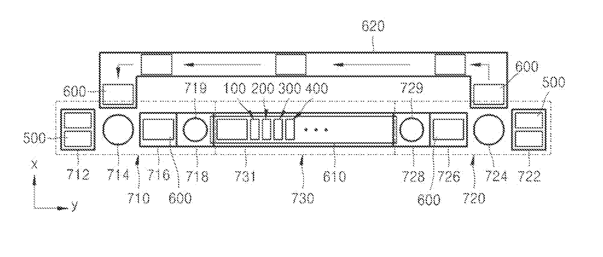
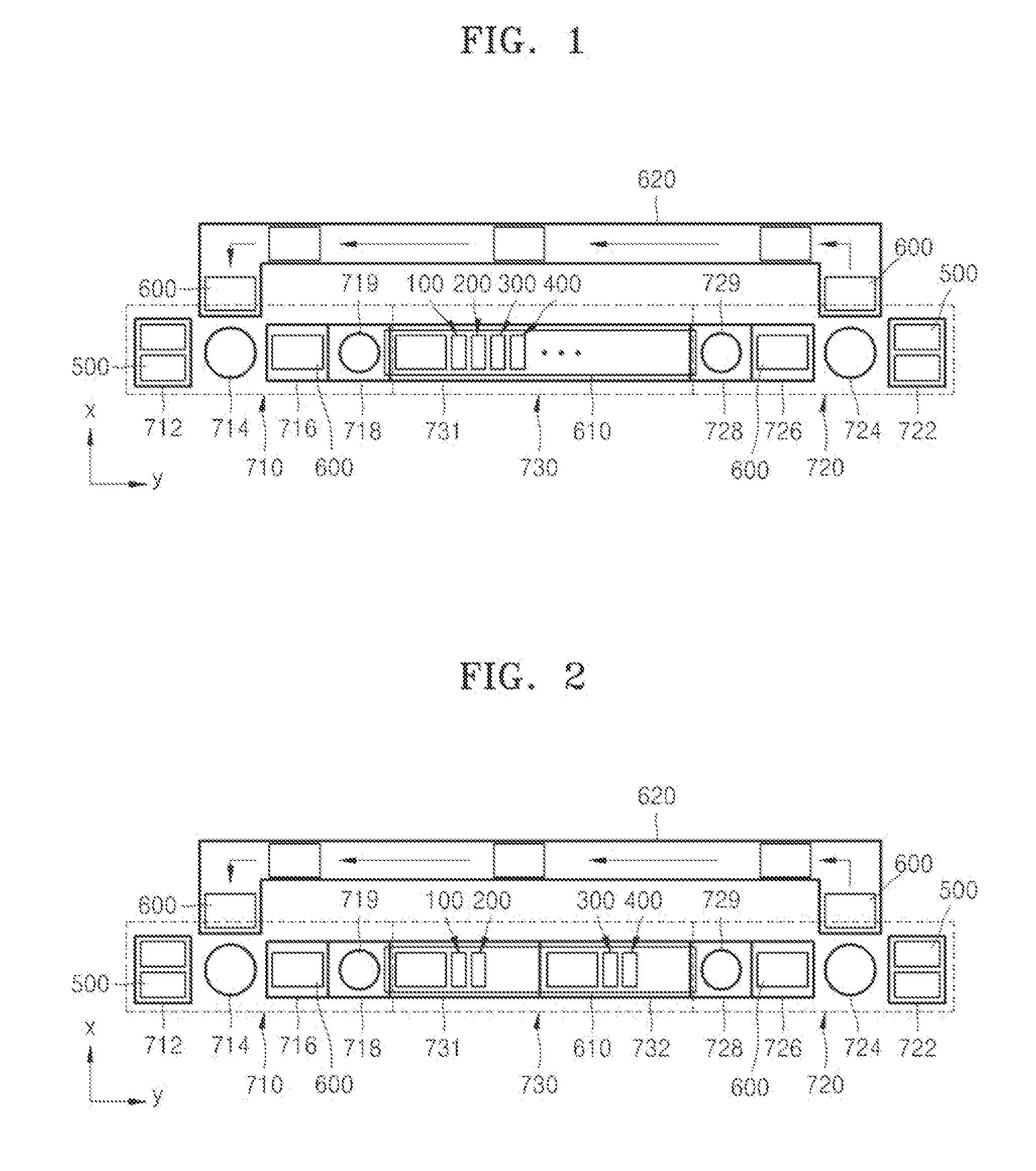
[0008]An aspect of the present invention provides a thin film deposition apparatus that may be easily manufactured, that may be easily used to manufacture large-sized display apparatuses on a mass scale and that allows high-definition patterning, and a method of manufacturing an organic light-emitting display apparatus by using the thin film deposition apparatus.
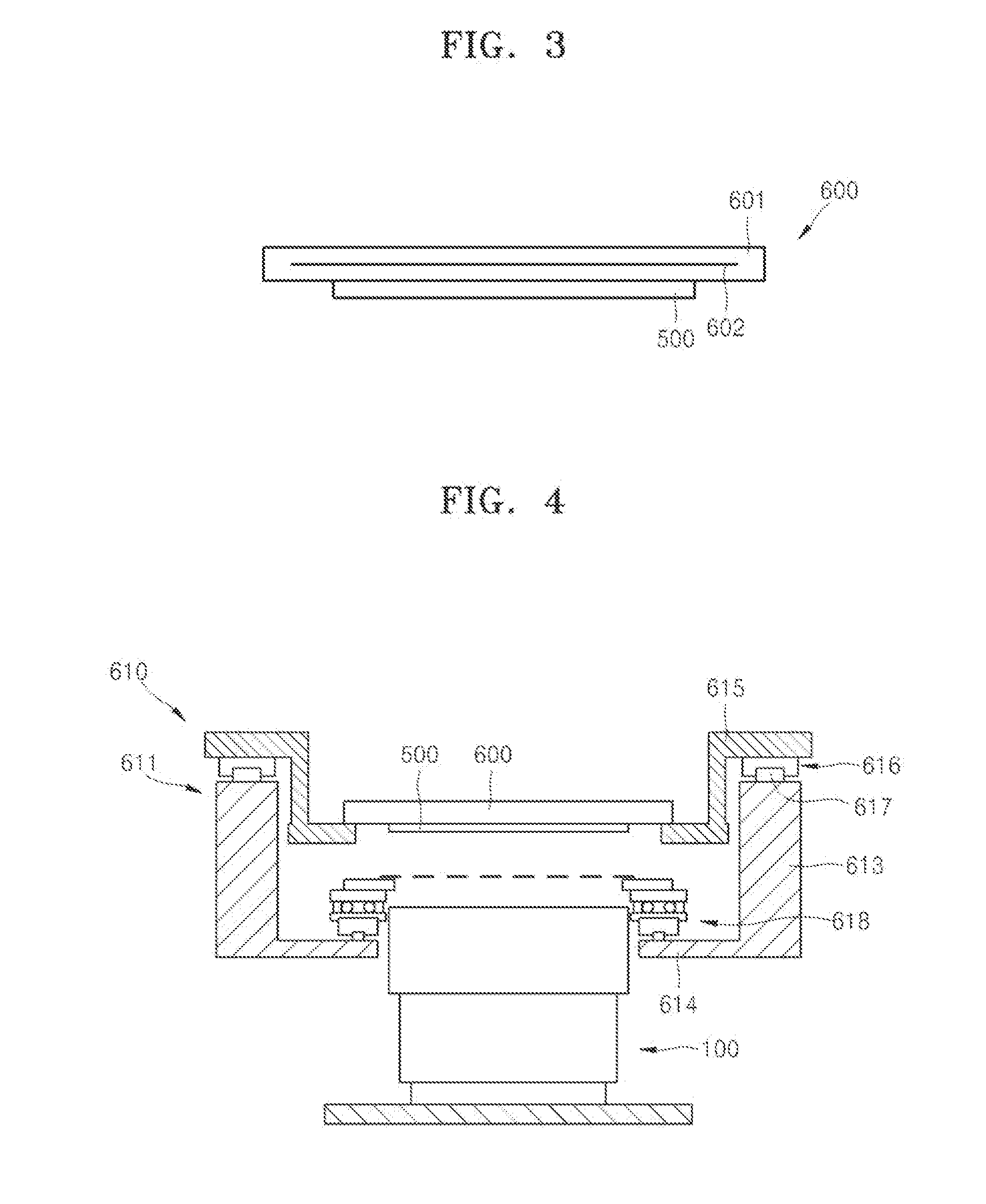
[0016]According to another aspect of the present invention, the connection member may seal a space between the deposition source and the deposition source nozzle unit, and the patterning slit sheet.

Problems solved by technology

However, when the FMM is used, it is not easy to form an organic thin film pattern on a large substrate, such as a mother glass having a large size.
In other words, when the large-sized mask is used, the mask may be bent due to self-gravity, and the organic thin film pattern may be distorted due to the bent mask.
This is not desirable for high definition patterning which is being increasingly used recently.

Method used


Image

  • Thin film deposition apparatus and method of manufacturing organic light-emitting display apparatus using the same
  • Thin film deposition apparatus and method of manufacturing organic light-emitting display apparatus using the same
  • Thin film deposition apparatus and method of manufacturing organic light-emitting display apparatus using the same

Examples


Embodiment Construction

[0063]Reference will now be made in detail to the present embodiments of the present invention, examples of which are illustrated in the accompanying drawings, wherein like reference numerals refer to the like elements throughout. The embodiments are described below in order to explain the present invention by referring to the figures.

[0064]The present invention will now be described more fully with reference to the accompanying drawings, in which exemplary embodiments of the invention are shown.

[0065]Here, when a first element is described as being coupled to a second element, the first element may be not be only directly coupled to the second element but may also be indirectly coupled to the second element via a third element. Moreover, it is to be understood that where is stated herein that one film or layer is “formed on” or “disposed on” a second layer or film, the first layer or film may be formed or disposed directly on the second layer or film or there may be intervening lay...


PUM

PropertyMeasurementUnit
Angleaaaaaaaaaa

Abstract

A thin film deposition apparatus used to manufacture large substrates on a mass scale and that allows high-definition patterning, and a method of manufacturing an organic light-emitting display apparatus using the same, the apparatus includes a loading unit fixing a substrate onto an electrostatic chuck; a deposition unit including a chamber maintained in a vacuum state and a thin film deposition assembly disposed in the chamber, separated from the substrate by a predetermined distance, to deposit a thin film on the substrate fixed on the electrostatic chuck; an unloading unit separating the substrate on which a deposition process is completed, from the electrostatic chuck; a first circulation unit sequentially moving the electrostatic chuck on which the substrate is fixed, to the loading unit, the deposition unit, and the unloading unit; and a second circulation unit returning the electrostatic chuck separated from the substrate to the loading unit from the unloading unit, wherein the first circulation unit passes through the chamber when passing through the deposition unit.

Description

CROSS-REFERENCE TO RELATED APPLICATIONS[0001]This application claims the benefit of Korean Patent Application Nos. 10-2009-0079765, filed on Aug. 27, 2009, and 10-2010-0011480, filed on Feb. 8, 2010, in the Korean Intellectual Property Office, the disclosures of which are incorporated herein in their entirety by reference.BACKGROUND[0002]1. Field[0003]An aspect of the present invention relates to a thin film deposition apparatus and a method of manufacturing an organic light-emitting display apparatus by using the same, and more particularly, to a thin film deposition apparatus that can be easily used to manufacture large substrates on a mass scale and that improves manufacturing yield, and a method of manufacturing an organic light-emitting display apparatus by using the thin film deposition apparatus.[0004]2. Description of the Related Art[0005]Organic light-emitting display apparatuses have a larger viewing angle, better contrast characteristics, and a faster response rate than o...

Claims


Application Information

Patent Timeline
IPC IPC(8): C23C16/52B05C11/00B05D3/00B05D5/00
CPCC23C14/042C23C14/12C23C14/243C23C14/246C23C14/568H01L21/67173H01L33/005H01L21/67236H01L21/6831H01L27/3211H01L51/001H01L51/0011H01L51/56H01L21/67225H10K59/35H10K71/164H10K71/166H10K71/441H10K71/231H10K71/00
Inventor JO, CHANG-MOGKIM, JONG-HEONCHOI, YONG-SUPKIM, SANG-SOOKANG, HEE-CHEOLCHOI, YOUNG-MOOK
Owner SAMSUNG DISPLAY CO LTD
Learn More