Boosting voltage levels applied to an access control line when accessing storage cells in a memory

Active Publication Date: 2011-03-17
ARM LTD
View PDF4 Cites 27 Cited by
  • Summary
  • Abstract
  • Description
  • Claims
  • Application Information

AI Technical Summary

Benefits of technology

[0010]The present invention recognises the problems of writing a data value to a semiconductor memory in systems where operational voltages and memory sizes are decreasing. It addresses this problem by providing a way of boosting the voltage level on an access control line during an access request and thereby increasing the chances of this voltage level being sufficient to trigger a change in data value if required. Furthermore, rather than providing a circuit for providing this boost for each access control line, with the attendant disadvantage of significantly increasing the area of the memory, it provides routing circuitry for routing the boost signal to a particular selected access control line, such that a boost signal can be generated for multiple access control lines and then routed to the appropriate one.
[0033]The problem of area scaling and voltage scaling makes the writing to the storage cells particularly problematic. Thus, this technique is particularly appropriate where the access request is a write request. However, there are some circumstances where it can be used for read requests as well. These circumstances may be where the stability of the cells are high and the performance of the read is important. An increase in voltage on the access control line during a read may make it more likely that the stored values in other cells are disturbed during the read but it also increases the speed of the read. Thus, in some circumstances it may be advantageous to provide the boost during the read.

Problems solved by technology

Furthermore, rather than providing a circuit for providing this boost for each access control line, with the attendant disadvantage of significantly increasing the area of the memory, it provides routing circuitry for routing the boost signal to a particular selected access control line, such that a boost signal can be generated for multiple access control lines and then routed to the appropriate one.
It should be noted that an optimal delay between the access request and the boost signal for a particular memory may in some cases be quite long and thus, the delay circuit needed to generate this delay may be quite large.

Method used


Image

  • Boosting voltage levels applied to an access control line when accessing storage cells in a memory
  • Boosting voltage levels applied to an access control line when accessing storage cells in a memory
  • Boosting voltage levels applied to an access control line when accessing storage cells in a memory

Examples


Embodiment Construction

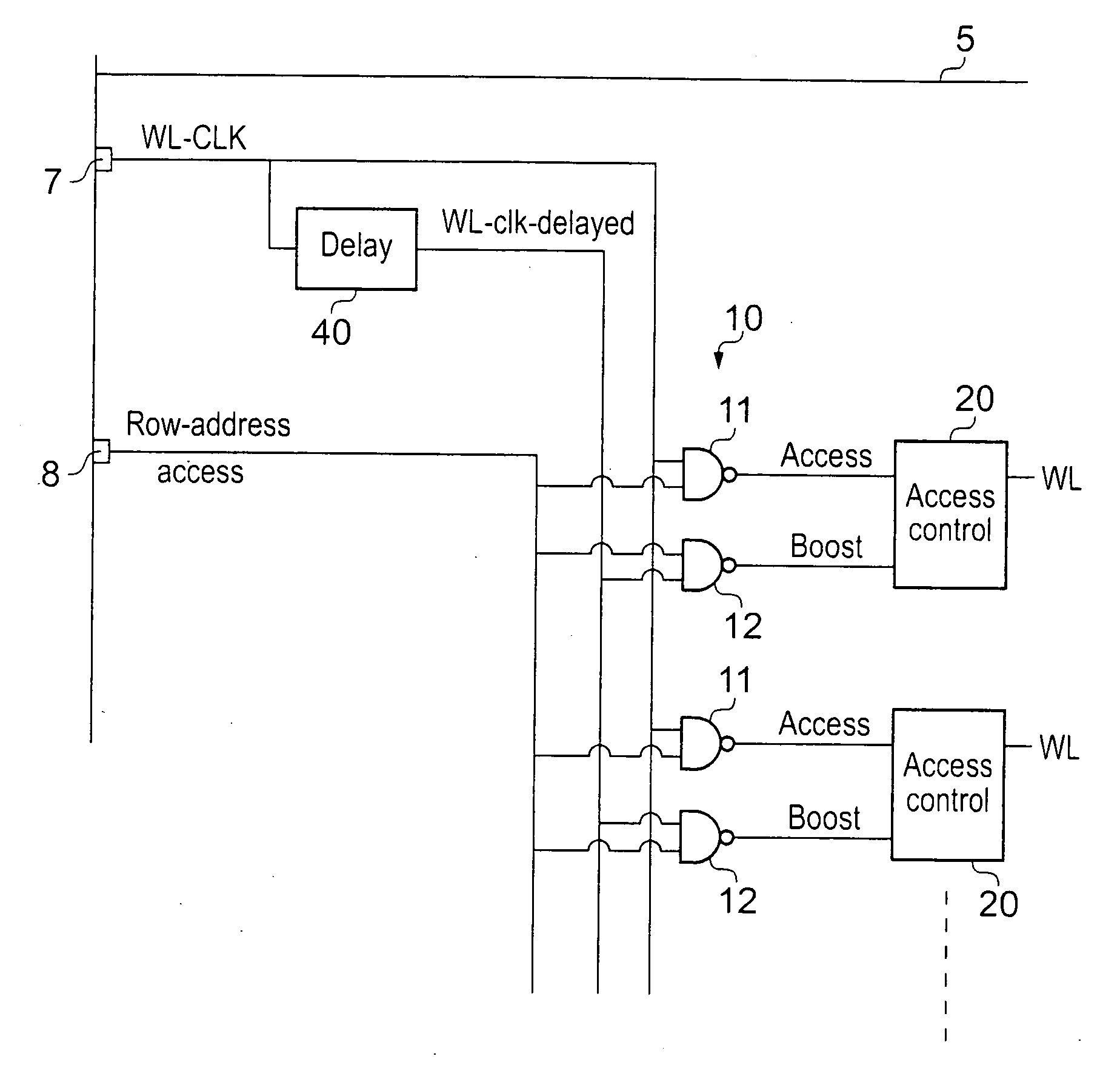
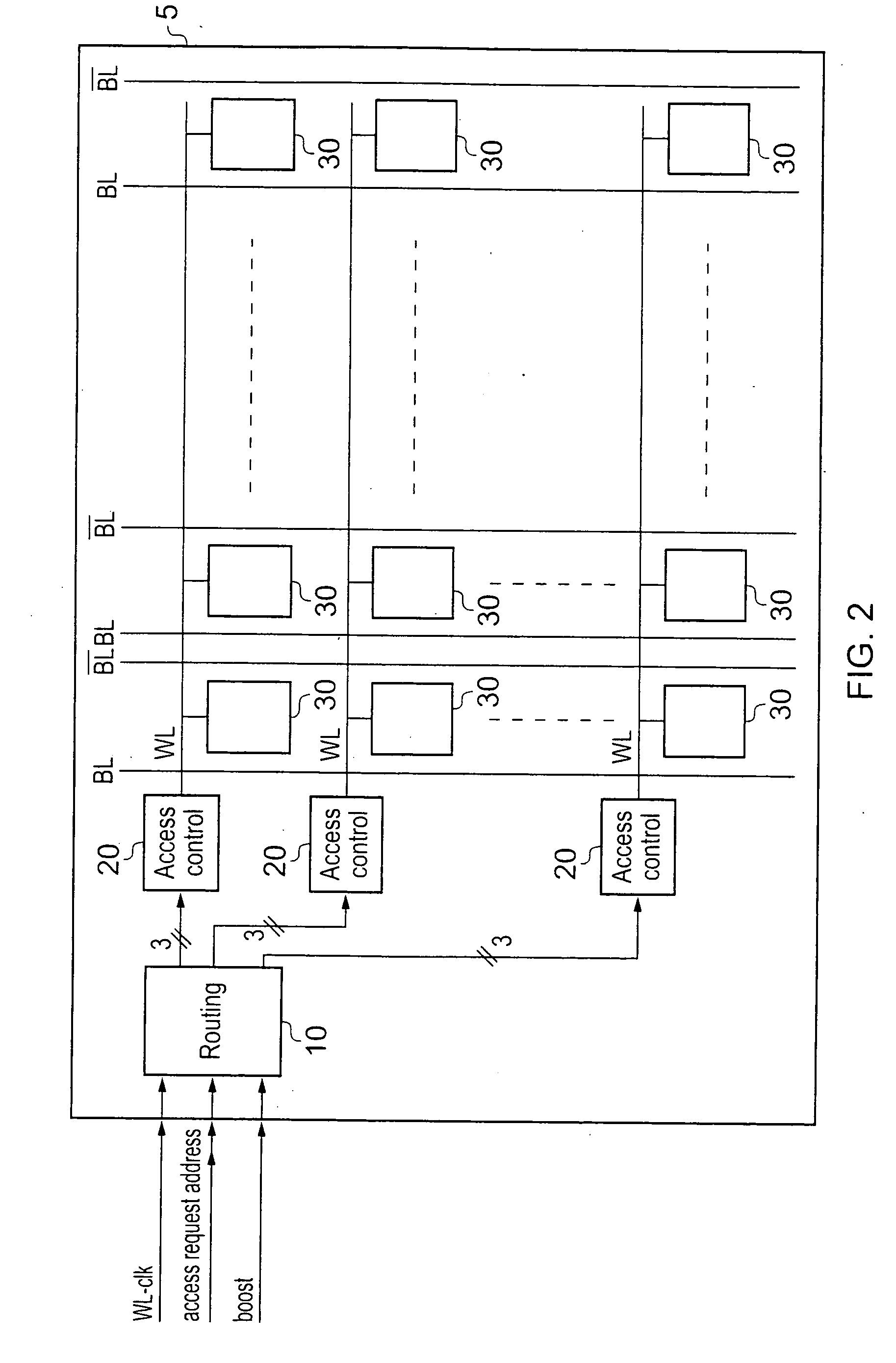
[0043]FIG. 2 shows a memory 5 according to an embodiment of the present invention. Memory 5 comprises a plurality of data storage cells 30 arranged in an array with requests to access data being made along a selected row of the array via word lines WL.

[0044]In response to an access request a word line for a row that contains the selected cell is fired to enable cells in that row to be accessed. Then the bit line and complementary bit line for the column that the selected cell is in are activated and a data value is read from or written to the cell depending on the access request.

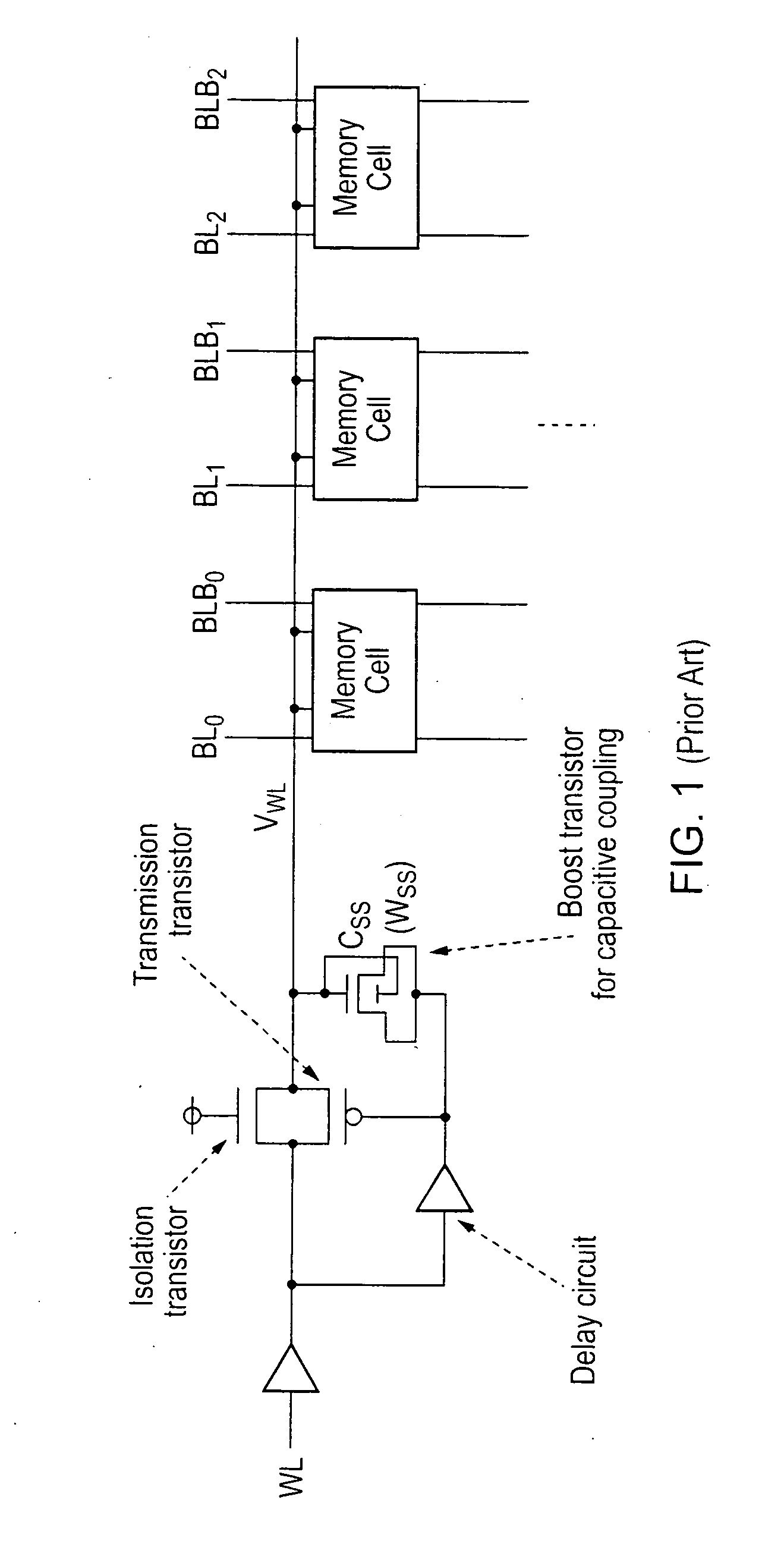
[0045]Access request signals for accessing particular storage cells are received from upstream processing logic in a data processing apparatus. In the case of the access request being a write request, then the write must be sufficient to switch the state stored in the cell if required and this may be difficult, particularly at low operating voltage levels. In order to ensure that the write is able to functio...


PUM


Abstract

A semiconductor memory storage device is disclosed, the memory comprises: a plurality of storage cells for storing data; at least two access control lines each for controlling access to a respective at least one of the plurality of storage cells; at least two access control circuits each for controlling a voltage level supplied to a corresponding one of the at least two access control lines in response to an access request, the at least two access control circuits each comprising a capacitor and switching circuitry; routing circuitry for routing the access request and a boost signal to a selected one of the at least two access control circuits in dependence upon an address associated with the access request; wherein the at least two access control circuits are each responsive to: receipt of the access request from the routing circuitry to connect the selected access control line to a supply voltage; and receipt of the boost signal from the routing circuitry to disconnect the supply voltage from the access control line and to couple the boost signal to the access control line through the capacitor of the access control circuit to provide a boost to a voltage level on the access control line.

Description

BACKGROUND OF THE INVENTION[0001]1. Field of the Invention[0002]The field of the invention relates to the field of data storage and in particular, to the storage and access of data in semiconductor memories.[0003]2. Description of the Prior Art[0004]With ever increasing demands to reduce both the size of devices and their power consumption, it is becoming increasingly challenging to design robust semiconductor memories such as SRAM. Each storage cell in an SRAM comprises a feedback loop for holding a data value. In order to write to the feedback loop and store a new value, the input data value must have a high enough voltage level to be able to switch the state stored by the feedback loop if required, while reading from the feedback loop should be performed without disturbing the values stored in any of the feedback loops.[0005]As dimensions scale down the variations in device properties due to random dopant fluctuations, line edge roughness etc. increase drastically.[0006]Thus, des...

Claims


Application Information

Patent Timeline
IPC IPC(8): G11C7/00G11C8/18
CPCG11C11/413G11C8/08
Inventor CHANDRA, VIKASPIETRZYK, CEZARYAITKEN, ROBERT CAMPBELL
Owner ARM LTD
Why Eureka
Try Eureka