

Photoelectric device, method of fabricating the same and packaging apparatus for the same
a technology of photoelectric devices and packaging apparatus, which is applied in the direction of electrical apparatus, semiconductor/solid-state device manufacturing, and semiconductor devices. it can solve the problems of high cost of led package b>100/b>, large manpower and extra assembly procedures, etc., and achieve the effect of improving the reliability and yield of photoelectric device production
- Summary
- Abstract
- Description
- Claims
- Application Information
AI Technical Summary
Benefits of technology
Problems solved by technology
Method used
Image

Examples
Embodiment Construction
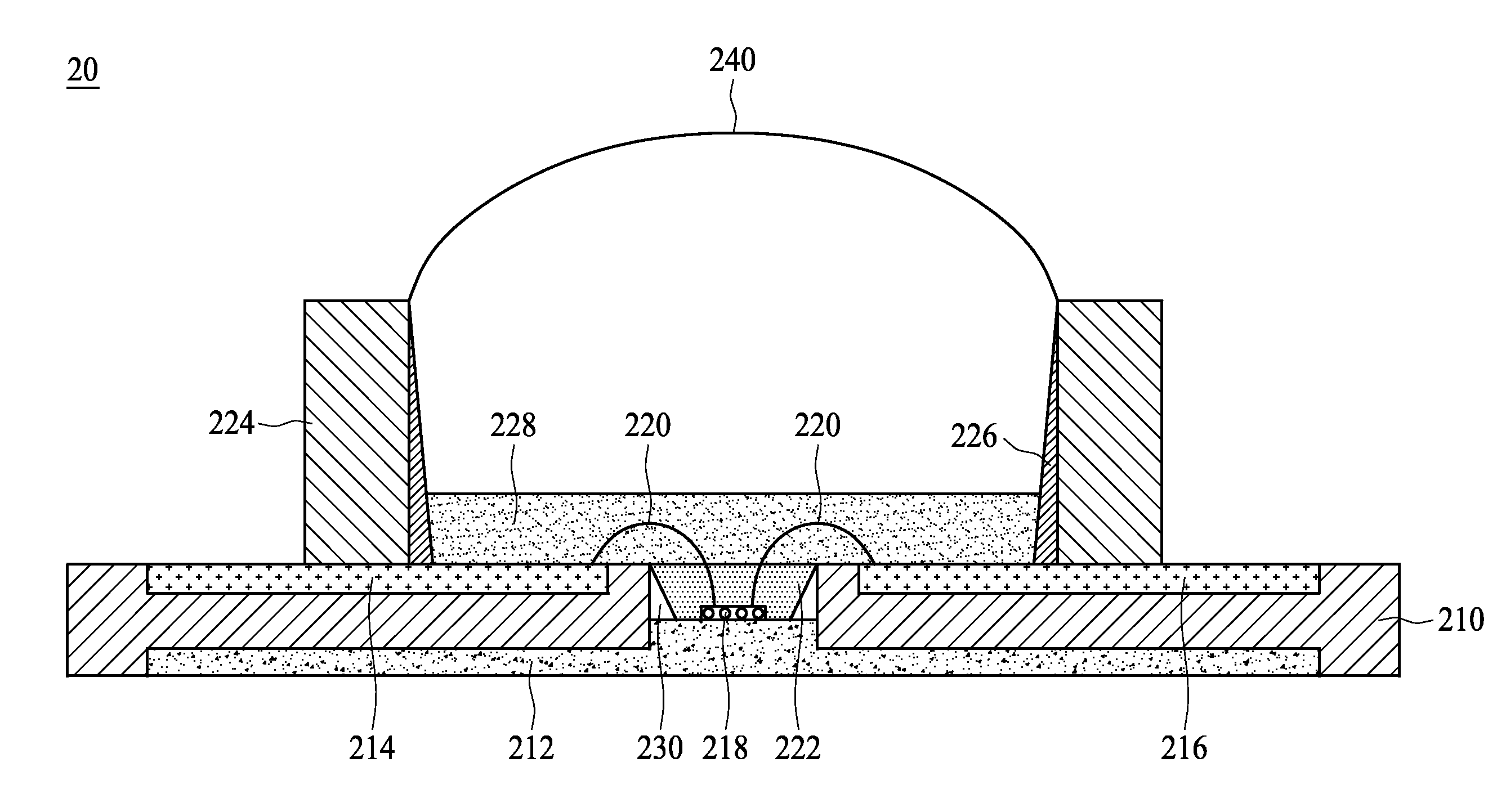
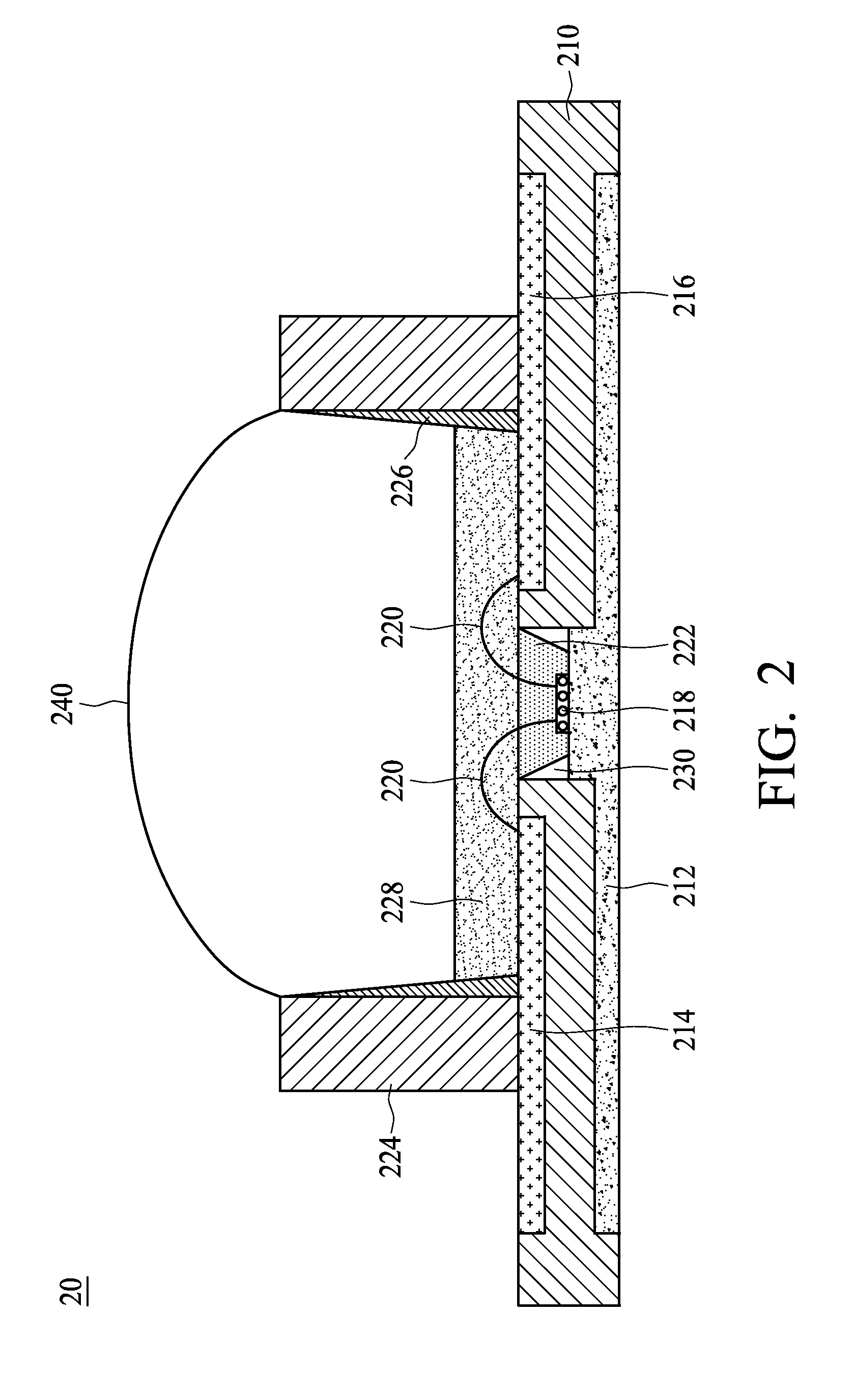
[0019]FIG. 2 is a cross-sectional view showing a photoelectric device 20 according to one embodiment of the present invention. The photoelectric device 20 adopts a ceramic substrate 210 as its substrate. The ceramic substrate 210 can be of high temperature co-fired ceramics or of low temperature co-fired ceramics. The ceramic substrate 210 is usually made of aluminum oxide; however, other material such as aluminum nitride (AlN), beryllium oxide (BeO), silicon carbide (SiC), glass, or diamond can be used to manufacture the ceramic substrate.
[0020]Referring to FIG. 2, the photoelectric device 20 comprises a thermal dissipation layer 212, a p-type electrode layer 214, and an n-type electrode layer 216, wherein the p-type electrode layer 214 and the n-type electrode layer 216 are able to electrically connect to an external power source (not shown). The thermal dissipation layer 212 may include any thermally conductive material, for example, metal. A photoelectric die 218 is disposed on ...
PUM
| Property | Measurement | Unit |
|---|---|---|
| thermal | aaaaa | aaaaa |
| brightness | aaaaa | aaaaa |
| physical size | aaaaa | aaaaa |
Abstract
Description
Claims
Application Information