Semiconductor device including vertical transistor and horizontal transistor and method of manufacturing the same

Active Publication Date: 2011-03-24
DENSO CORP
View PDF9 Cites 52 Cited by
  • Summary
  • Abstract
  • Description
  • Claims
  • Application Information

AI Technical Summary

Benefits of technology

In view of the foregoing problems, it is an object of the present invention to provide a semiconductor device that can restrict a change in electric properties of a

Problems solved by technology

Especially in a case where the vertical transistors form a power section for electric power and the horizontal transistors form a control section for driving the power sec

Method used


Image

  • Semiconductor device including vertical transistor and horizontal transistor and method of manufacturing the same
  • Semiconductor device including vertical transistor and horizontal transistor and method of manufacturing the same
  • Semiconductor device including vertical transistor and horizontal transistor and method of manufacturing the same

Examples


first embodiment

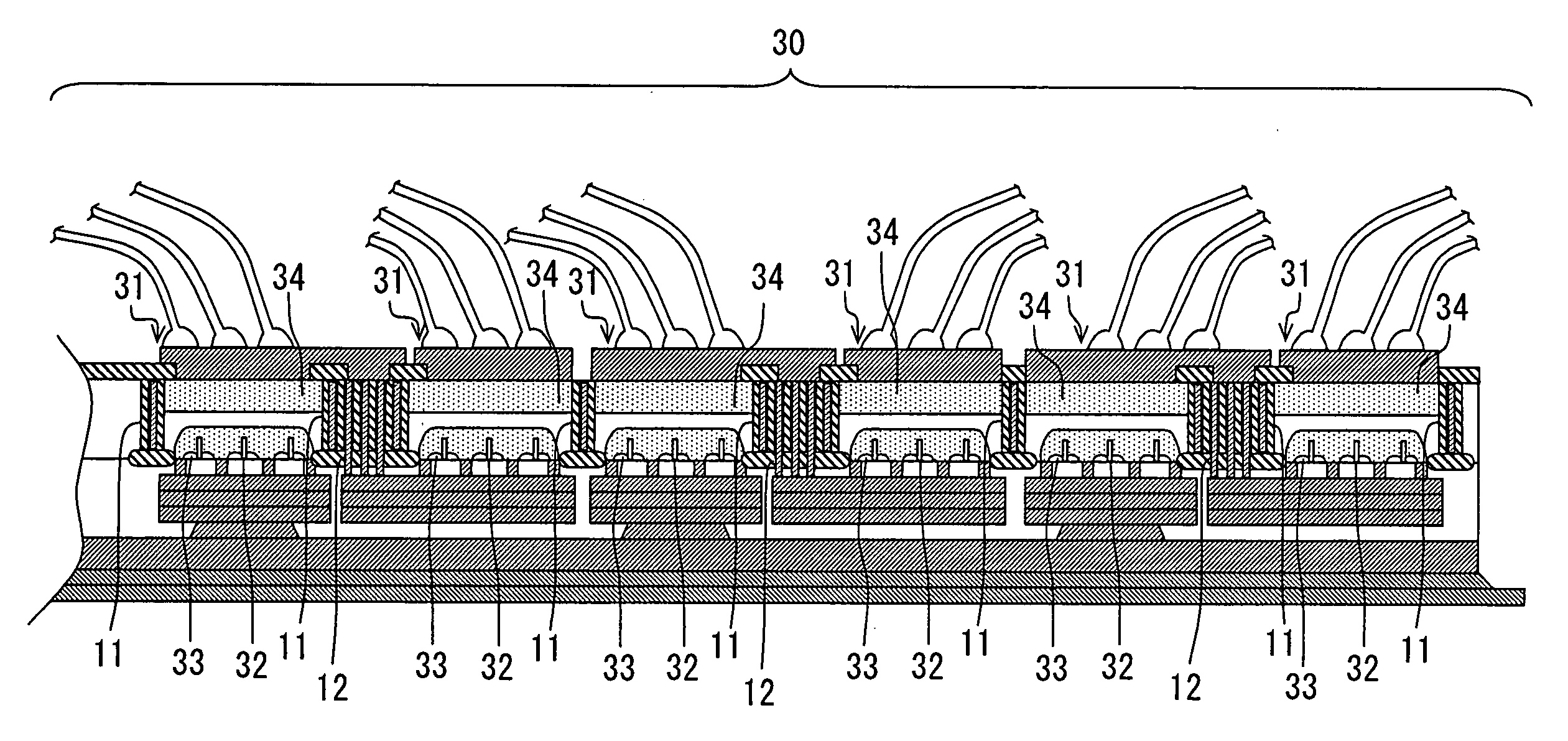
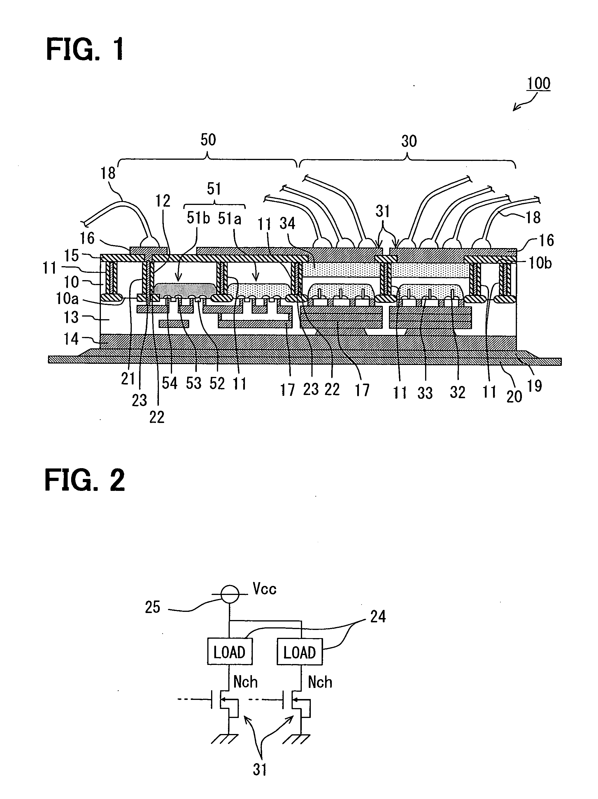
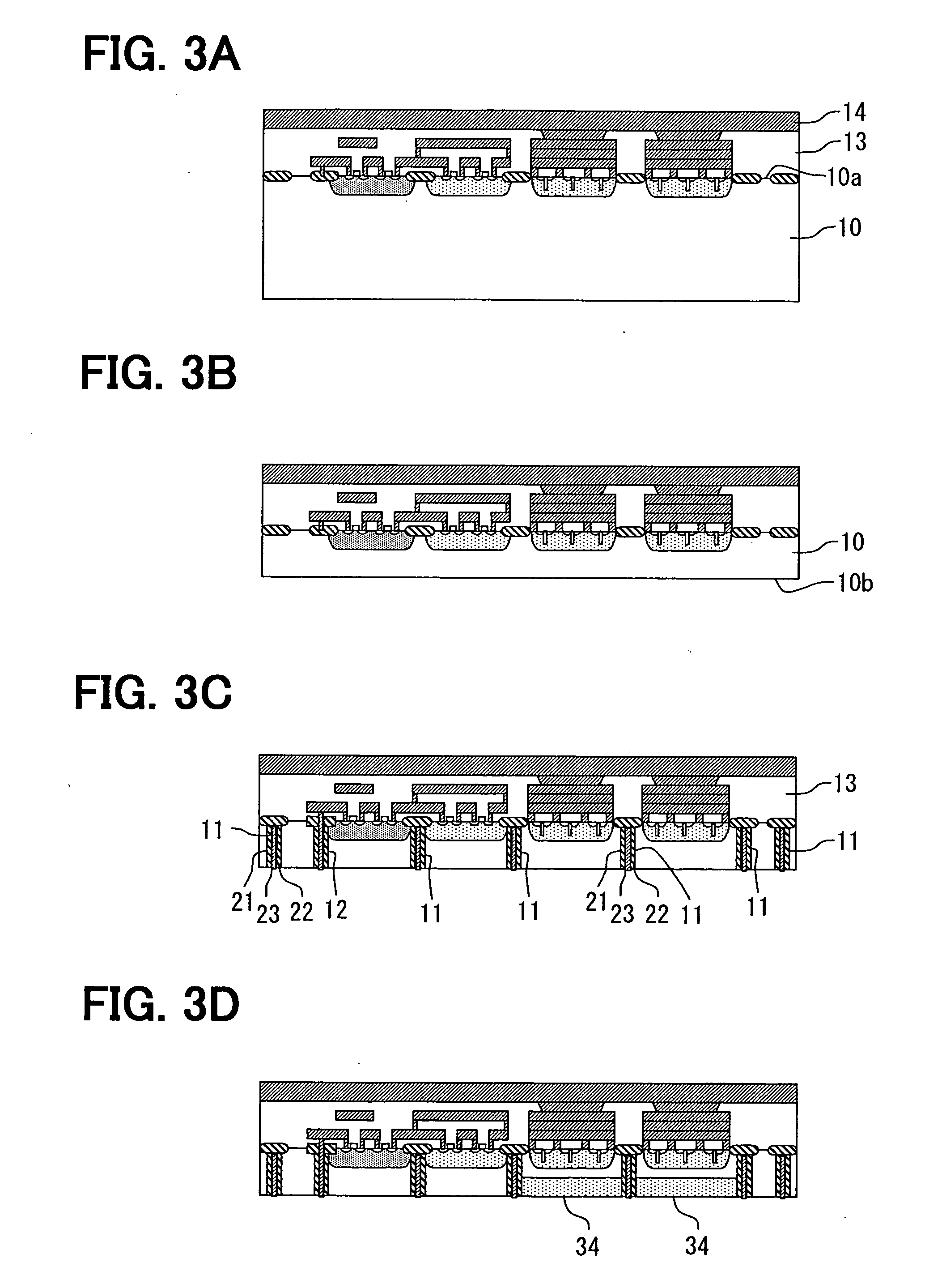
A semiconductor device 100 according to a first embodiment of the present invention will be described with reference to FIG. 1 to FIG. 5D.

As shown in FIG. 1, the semiconductor device 100 includes a semiconductor substrate 10, a power section 30, and a control section 50. The power section 30 and the control section 50 are formed in the semiconductor substrate 10. The power section 30 includes a plurality of vertical MOSFETs 31. The control section 50 includes a plurality of horizontal MOSFETs 51.

The semiconductor substrate 10 has a plurality of isolation trenches 11. The isolation trenches 11 divide the semiconductor substrate 10 into a plurality of element-forming regions that are electrically separated from each other. In each of the element forming regions, the vertical MOSFET 31 or the horizontal MOSFET 51 is formed. In the present embodiment, all the vertical MOSFETs 31 are N-channel type MOSFETs. The horizontal MOSFETs 51 are a complementary MOSFET including an N-channel type ...

second embodiment

A semiconductor device 100 according to a second embodiment of the present invention will be described with reference to FIG. 6 and FIG. 7.

Because the semiconductor device 100 according to the present embodiment have many portions in common with the semiconductor device 100 according to the first embodiment, a description of the common portions will be omitted and different portions will be mainly described. In the following description, the same reference numbers are given to components same as the components described in the first embodiment. The control section 50 in the semiconductor device 100 according to the present embodiment is similar to the control section 50 in the semiconductor device 100 according to the first embodiment. Thus, a description of the control section 50 will be omitted.

In the semiconductor device 100 according to the present embodiment, the vertical MOSFETs 31 are a complementary MOSFET including an N-channel type MOSFET 31a and a P-channel type MOSFET 31...

third embodiment

A semiconductor device 100 according to a third embodiment of the present invention will be described with reference to FIG. 10 and FIG. 11.

Because the semiconductor device 100 according to the present embodiment has many portions in common with the semiconductor device 100 according to the first embodiment or the semiconductor device 100 according to the second embodiment, a description of the common portions will be omitted and different portions will be mainly described. In the following description, the same reference numerals are given to components same as the components described in the first embodiment and the second embodiment. The control section 50 in the semiconductor device 100 according to the present embodiment is similar to the control section 50 in the semiconductor device 100 according to the first embodiment. Thus, a description of the control section 50 will be omitted.

The semiconductor device 100 according to the present embodiment includes three pairs of N-chan...


PUM


Abstract

A semiconductor device includes a semiconductor substrate, a vertical transistor, a horizontal transistor, a lead, wire-bonding pads, and penetrating electrodes. The semiconductor substrate has first and second surfaces and includes a first surface portion adjacent to the first surface. The vertical transistor includes first and second electrodes on the first surface and a third electrode on the second surface. The horizontal transistor includes first, second, and third electrodes on the first surface. The vertical transistor and the horizontal transistor further include PN junction parts in the first surface portion. The lead is disposed to the first surface and is electrically coupled with the first electrode of the vertical transistor. The wire-bonding pads are disposed on the second surface. The second electrode of the vertical transistor and the first to third electrodes of the horizontal transistor are electrically coupled with the wire-boding pads through the penetrating electrodes.

Description

CROSS REFERENCE TO RELATED APPLICATIONSThe present application is based on and claims priority to Japanese Patent Application No. 2009-218324 filed on Sep. 23, 2009, the contents of which are incorporated in their entirety herein by reference.BACKGROUND OF THE INVENTION1. Field of the InventionThe present invention relates to a semiconductor device including a vertical transistor and a horizontal transistor. The present invention also relates to a method of manufacturing the semiconductor device.2. Description of the Related ArtUS 2008 / 0135932 A (corresponding to JP-A-2008-166705) discloses a semiconductor device in which a semiconductor substrate is divided into a plurality of field areas by a plurality of isolation trenches. In at least one of the field areas, a double-sided electrode element having electrodes on both sides of the semiconductor substrate is formed. In at least another one of the field areas, a single-sided electrode element having a pair of electrodes on one side ...

Claims


Application Information

Patent Timeline
IPC IPC(8): H01L27/088H01L21/28
CPCH01L21/823487H01L2924/00014H01L24/05H01L24/06H01L24/49H01L27/088H01L2224/04042H01L2224/05556H01L2224/05599H01L2224/0603H01L2224/48463H01L2224/49111H01L2224/494H01L2224/85399H01L2924/01004H01L2924/01005H01L2924/01015H01L2924/01029H01L2924/01082H01L2924/13055H01L2924/13091H01L23/481H01L2924/1305H01L2924/1306H01L2224/73265H01L2924/01033H01L2924/01006H01L24/48H01L2224/45099H01L2924/00H01L2924/12036H01L2924/00012
Inventor KITAMURA, YASUHIRO
Owner DENSO CORP
Why Eureka
Try Eureka