Semiconductor structures and methods for forming isolation between fin structures of finfet devices

a technology of semiconductor structures and fin structures, applied in the direction of semiconductor devices, electrical equipment, basic electric elements, etc., can solve the problems of difficult control, affecting the thickness of the dielectric layer, and difficult to isolate the fin structure on a bulk silicon wafer, so as to reduce the variability of the height of the fin

Active Publication Date: 2011-03-24
GLOBALFOUNDRIES US INC
View PDF6 Cites 67 Cited by
  • Summary
  • Abstract
  • Description
  • Claims
  • Application Information

AI Technical Summary

Benefits of technology

[0011]In accordance with another exemplary embodiment, a method for forming isolation between fin structures formed from a bulk silicon wafer comprises the step of providing a bulk silicon wafer having one or more fin structures formed therefrom with isolation trenches between the one or more fin structures and each of the fin structures having vertical sidewalls. An oxide layer is deposited in the bottom of each of the isolation trenches of the bulk silicon wafer and on the vertical sidewalls of the one or more fin structures using a high density plasma chemical vapor deposition (HDPCVD) process. The oxide layer is isotropically etched from the vertical sidewalls and at least a portion thereof is isotropically etched from the isolation trenches to form an isolating oxide layer in the bottom of the isolation trenches of substantially uniform thickness that forms isolation between the fin structures and substantially reduces fin height variability.

Problems solved by technology

Isolating fin structures on a bulk silicon wafer is especially problematic as the silicon of the bulk silicon wafer between the fin structures forms a conduction path.
This conventional technique is difficult to control, often resulting in a dielectric layer that varies in thickness.
The filling of high aspect ratio isolation trenches is difficult.
Even state of the art oxide chemical vapor deposition (CVD) processes such as advanced high density plasma (HDP) or ozone based TEOS (tetraethylorthosilicate) processes cannot reliably fill these high aspect ratio isolation trenches.
This causes problems in controlling and creating electrical isolation in FinFET devices.
Additionally, bulk silicon wafers lack an etch stop layer upon which etching of the fin can terminate.
Without this etch stop layer, variability in the etch depth results in variability in the fin height.

Method used


Image

  • Semiconductor structures and methods for forming isolation between fin structures of finfet devices
  • Semiconductor structures and methods for forming isolation between fin structures of finfet devices
  • Semiconductor structures and methods for forming isolation between fin structures of finfet devices

Examples


Embodiment Construction

[0018]The following detailed description of the invention is merely exemplary in nature and is not intended to limit the invention or the application and uses of the invention. Furthermore, there is no intention to be bound by any theory presented in the preceding background of the invention or the following detailed description of the invention.

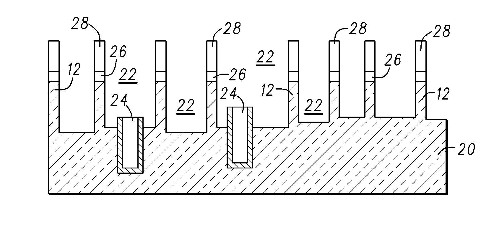
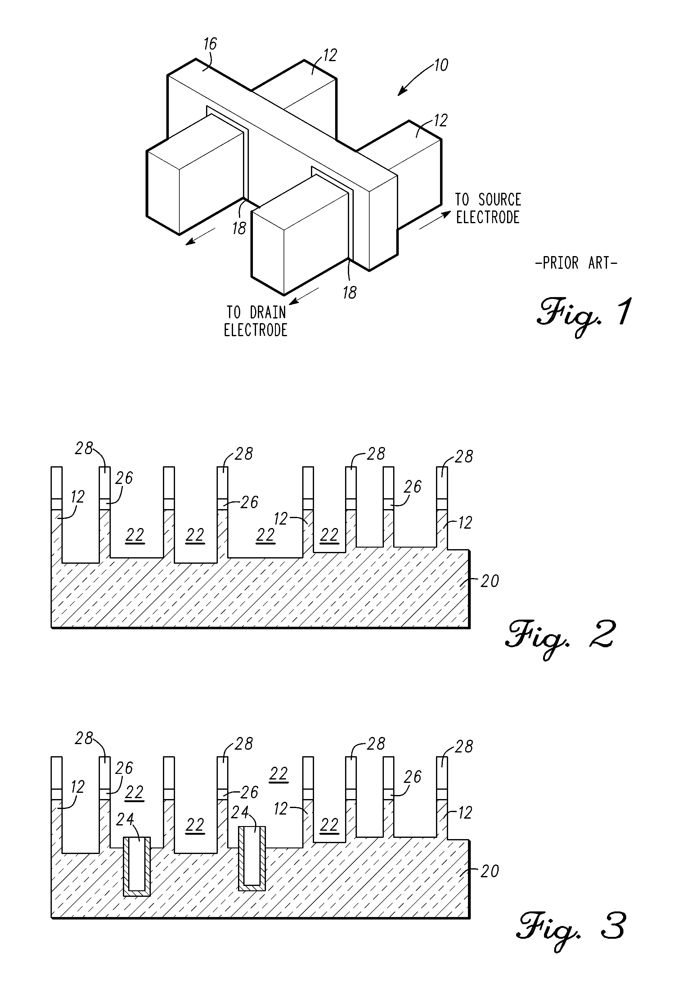
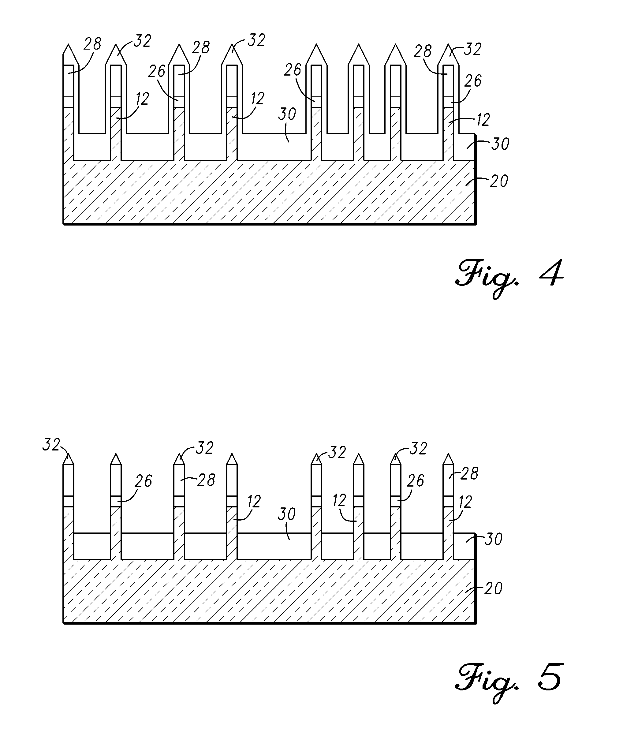
[0019]Methods in accordance with exemplary embodiments of the present invention are provided for forming isolation between one or more previously-formed fin structures 12 on a bulk silicon wafer 20. The step of forming the one or more fin structures defines isolation trenches 22 on the exposed bulk silicon wafer 20 between the one or more previously-formed fin structures. The fin structures 12 include vertical sidewalls.

[0020]Fin structures are typically formed using conventional photolithographic or anisotropic etching processes (e.g., reactive ion etching (RIE) or the like), however, it will be understood that the present invention is not ...


PUM


Abstract

Semiconductor structures and methods for forming isolation between fin structures formed from a bulk silicon wafer are provided. A bulk silicon wafer is provided having one or more fin structures formed therefrom. Forming of the fin structures defines isolation trenches between the one or more fin structures. Each of the fin structures has vertical sidewalls. An oxide layer is deposited in the isolation trenches and on the vertical sidewalls using HPDCVD in about a 4:1 ratio or greater. The oxide layer is isotropically etched to remove the oxide layer from the vertical sidewalls and a portion of the oxide layer from the bottom of the isolation trenches. A substantially uniformly thick isolating oxide layer is formed on the bottom of the isolation trench to isolate the one or more fin structures and substantially reduce fin height variability.

Description

FIELD OF THE INVENTION[0001]The present invention generally relates to semiconductor structures and methods for fabricating semiconductor structures, and more particularly relates to methods for fabricating bulk FinFET devices having shallow trench isolation (STI).BACKGROUND OF THE INVENTION[0002]In contrast to traditional planar metal-oxide-semiconductor field-effect transistors (MOSFETS), which are fabricated using conventional lithographic fabrication methods, nonplanar FETs (field-effect transistors) incorporate various vertical transistor structures, and typically include two or more gate structures formed in parallel. One such semiconductor structure is the “FinFET” which takes its name from the multiple thin silicon “fins” that are used to form the respective gate channels, and which are typically on the order of tens of nanometers in width.[0003]More particularly, referring to the exemplary prior art nonplanar MOS transistor having a FinFET configuration shown in FIG. 1, a F...

Claims


Application Information

Patent Timeline
Patent Type & Authority Applications(United States)
IPC IPC(8): H01L29/06H01L21/762
CPCH01L21/76229H01L29/7851H01L29/66795
Inventor KNORR, ANDREASJOHNSON, FRANK SCOTT
Owner GLOBALFOUNDRIES US INC
Why Eureka
Try Eureka